Introduction
Surface mount current sensors play a critical role in modern electronics where space constraints demand precise current measurement without compromising performance. These components, often referred to as SMD current sensors, enable surface mount current sensing directly on high density PCBs, supporting applications in power supplies, motor drives, and battery management systems. As electronic devices shrink, engineers face the challenge of integrating miniature current sensors while maintaining accuracy and reliability during assembly processes like reflow soldering. Miniaturization strategies focus on reducing package sizes and optimizing PCB layouts to fit more functionality into limited board real estate. This article explores practical approaches to implementing these sensors in high density PCB assemblies, addressing common troubleshooting issues along the way. By following established guidelines, designers can avoid pitfalls such as soldering defects and signal noise.
What Are Surface Mount Current Sensors and Why Do They Matter?
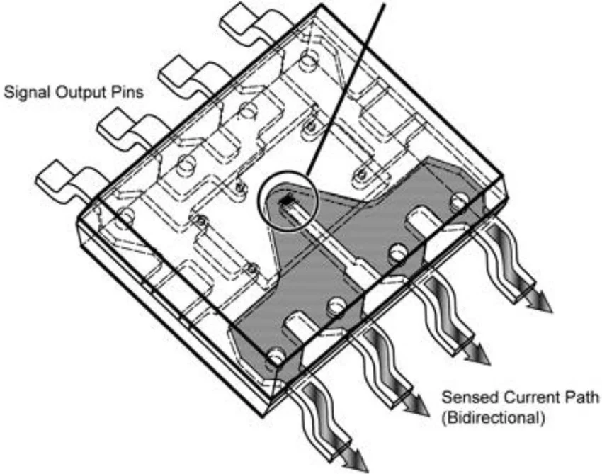
Surface mount current sensors are compact devices designed for direct attachment to PCB surfaces, measuring current flow through conductive paths using principles like the Hall effect or resistive shunts. Unlike traditional through-hole sensors, SMD current sensors eliminate the need for extra board space and vias, making them ideal for high density PCB designs where component density exceeds conventional limits. They provide real-time feedback for overcurrent protection, efficiency monitoring, and control loops in compact systems. The shift toward miniature current sensors addresses the growing demand for smaller form factors in consumer electronics, automotive modules, and industrial controls. Reliability suffers if miniaturization overlooks factors like thermal dissipation or electromagnetic interference, leading to field failures. Engineers must prioritize sensors compatible with automated assembly to ensure scalability in production.
In high density PCB assemblies, these sensors contribute to overall system miniaturization by reducing trace lengths and parasitic inductance. Troubleshooting early integration issues, such as offset drift in small packages, prevents costly rework. Their matter lies in enabling higher power densities without proportional board size increases.
Technical Principles of SMD Current Sensors
SMD current sensors primarily operate on magnetic field detection or voltage drop measurement across a sense element. Hall effect types generate a voltage proportional to the magnetic field produced by the current, offering galvanic isolation ideal for high voltage applications. Resistive shunt variants use low-value surface mount resistors where the voltage drop directly correlates to current, providing simplicity but introducing power loss. Coreless designs eliminate bulky magnetic cores, allowing further package shrinkage while maintaining bandwidth for fast transients. Each type suits specific needs, with Hall-based sensors excelling in AC/DC measurement and shunts in low-cost DC sensing. Understanding these mechanisms helps in selecting the right sensor for high density environments.
Miniaturization at the sensor level involves shrinking the die and packaging to ultra-small footprints, often under 5mm in length. This reduction amplifies challenges like sensitivity to external fields and temperature coefficients. PCB integration strategies embed sense elements within traces, bypassing discrete components entirely for ultimate density. Noise coupling becomes a key troubleshooting focus, as tight layouts increase crosstalk risks.
Miniaturization Strategies for High-Density PCB Integration
Selecting sensors with progressively smaller packages, such as from standard SOIC to DFN or WSON, forms the foundation of miniaturization. These miniature current sensors fit between fine-pitch BGAs and passives, maximizing board utilization in high density PCBs. Designers should verify package coplanarity to avoid bridging during placement. Combining this with HDI structures like microvias allows stacking layers for routing flexibility. Thermal management requires vias under the sensor to wick heat away, preventing gain errors from self-heating. Practical tip: simulate junction temperatures early to identify hotspots.
Another strategy embeds current sensing into PCB traces using widened sections as shunts, eliminating discrete SMD current sensors where space is premium. Kelvin connections, with separate force and sense traces, ensure accurate four-wire measurement despite trace resistances. This approach suits high density PCB assemblies but demands precise etching control for uniformity. Troubleshooting trace variations involves calibration routines post-assembly. Hybrid methods pair trace shunts with nearby amplifiers in tiny packages for signal conditioning.
Reflow soldering current sensors demands attention to moisture sensitivity, as smaller encapsulants absorb vapor faster. Pre-baking and dry storage mitigate popcorn effects during peak reflow temperatures. Fine-pitch leads risk tombstoning if stencil apertures are mismatched.
Best Practices for PCB Layout and Assembly
Land pattern design per IPC-7351B guidelines ensures optimal solder joint formation for SMD current sensors. Choose density levels matching assembly capabilities, with most level B or C patterns suiting high density PCBs. Toe and heel fillet dimensions guide stencil thickness, typically 0.1mm for fine pitch. Misaligned patterns lead to open joints, troubleshootable via X-ray inspection. Verify courtyard keepouts to prevent adjacent component interference.
For surface mount current sensing, route sense traces as differential pairs with matched lengths to minimize common-mode noise. Guard traces shield against EMI in crowded high density layouts. Ground planes under the sensor reduce loop inductance, but slots prevent eddy currents from skewing readings. Simulate parasitics using field solvers for validation. Placement near the current path cuts trace drops, enhancing accuracy.
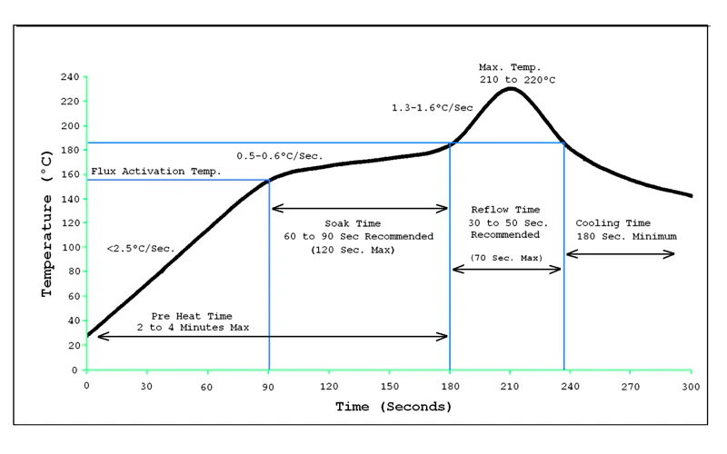
Reflow profiles must align with sensor classifications under IPC/JEDEC J-STD-020F to avoid delamination. Ramp up slowly to 150 degrees Celsius for preheat, holding to evaporate flux volatiles. Peak temperatures around 260 degrees Celsius for lead-free solders test package robustness. Cool-down rates below 6 degrees per second prevent warping. Monitor with thermocouples on test coupons mimicking production boards. Post-reflow AOI catches bridges or voids early.
Thermal vias arrays, filled and plated, dissipate power from miniature current sensors effectively. Fan-out high-current paths using IPC-2221C trace width charts to handle sensed currents without excessive voltage drops. Layer stacking influences crosstalk; dedicate inner planes for returns.
Troubleshooting Common Issues in Miniaturized Assemblies
Tombstoning plagues reflow soldering current sensors on uneven pads, often from rapid wetting differences. Balance stencil openings at 80-90% of pad area and use low-residue pastes. Solder balls arise from flux splash; optimize squeegee pressure and speed. Head-in-pillow defects signal paste volume issues, fixed by finer apertures.
Accuracy drifts in high density PCBs stem from thermal gradients or stray fields. Isolate sensors with mu-metal shields if needed, though rare in SMD form. Offset calibration via software compensates manufacturing variances. Vibration testing reveals mechanical weaknesses in tiny packages.
Yield drops correlate with handling; ESD controls and MSL-rated storage are non-negotiable.
Conclusion
Miniaturization strategies for SMD current sensors enable high density PCB assemblies by prioritizing small packages, precise layouts, and robust assembly processes. Key practices include IPC-standard land patterns, controlled reflow profiles, and noise-mitigating routing to ensure reliable surface mount current sensing. Troubleshooting soldering defects and thermal issues upfront boosts yields and longevity. Engineers achieve compact, high-performance designs by balancing density with manufacturability. Future trends point to even smaller integrated solutions, demanding ongoing adherence to evolving standards.
FAQs
Q1: What are the main advantages of SMD current sensors in high density PCB designs?
A1: SMD current sensors offer compact footprints that fit seamlessly into high density PCBs, reducing overall board size while providing accurate surface mount current sensing. They support automated assembly for high-volume production and minimize parasitics for better signal integrity. Troubleshooting is simpler with standard reflow processes, and isolation variants enhance safety in power circuits. These benefits drive efficiency in space-constrained applications like wearables and automotive electronics.
Q2: How do you ensure reliable reflow soldering for current sensors?
A2: Follow IPC/JEDEC J-STD-020F classifications to bake out moisture before reflow soldering current sensors, using dry nitrogen ovens if needed. Optimize profiles with preheat soaks and controlled peaks to prevent voids or cracks. Use laser-cut stencils for precise paste deposition on miniature pads. Post-reflow inspect with AOI and shear testing for joint strength. This approach minimizes defects in high density assemblies.
Q3: What challenges arise with miniature current sensors and how to troubleshoot them?
A3: Miniature current sensors suffer noise from nearby traces and thermal drift in high density PCBs; mitigate with twisted pairs and heat sinks. Soldering issues like bridging occur due to fine pitch, resolved by finer stencils and flux selection. Calibrate for offsets post-assembly. Simulate layouts to predict issues early. These steps ensure consistent performance.
Q4: Why follow standards like IPC-7351B for surface mount current sensing layouts?
A4: IPC-7351B provides verified land patterns for SMD current sensors, optimizing solder joints and rework clearances in high density PCB designs. It standardizes densities for manufacturability, reducing variability across fabs. Proper adherence prevents opens or shorts, streamlining troubleshooting. This fosters reliable surface mount current sensing without custom iterations.
References
IPC-7351B — Generic Requirements for Surface Mount Design and Land Pattern Standard. IPC, 2010
IPC/JEDEC J-STD-020F — Moisture/Reflow Sensitivity Classification for Non-Hermetic Surface Mount Devices. IPC/JEDEC, 2023
IPC-2221C — Generic Standard on Printed Board Design. IPC, 2023