Introduction
In the intricate ecosystem of Printed Circuit Board Assembly (PCBA), soldering is not merely a mechanical attachment process; it is the fundamental mechanism that ensures the electrical integrity and mechanical reliability of electronic devices. As electronic components shrink in size while increasing in complexity—driven by the demands of IoT, automotive electronics, and aerospace applications—the methodology used to form solder joints has become a critical strategic decision for manufacturers.
This comprehensive guide explores the spectrum of modern soldering methodologies. We will analyze the industrial efficacy of Wave Soldering, the precision of Selective Soldering, and the indispensable role of Manual Soldering in specialized environments. Furthermore, we will delve into the rigorous protocols for troubleshooting and defect mitigation based on IPC-A-610 and J-STD-001 standards, providing a holistic view of the soldering landscape.
Advantages and Disadvantages of Wave Soldering Machines
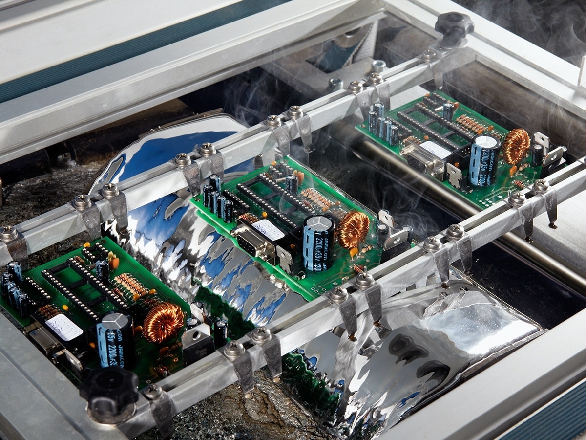
For decades, wave soldering has remained the cornerstone of mass production, particularly for Printed Circuit Boards (PCBs) utilizing Through-Hole Technology (THT). The process relies on a deceptively simple premise: passing the PCB over a pumped wave of molten solder. However, the thermodynamics and fluid dynamics involved require precise engineering control.
The Mechanism of Mass Production
The efficacy of wave soldering lies in its ability to solder hundreds, potentially thousands, of joints simultaneously. The process typically involves four distinct stages:
- Fluxing: Removing surface oxides and reducing surface tension.
- Preheating: Activating the flux and mitigating thermal shock.
- Wave Contact: The formation of the intermetallic bond.
- Cooling: Stabilizing the grain structure of the solder joint.
Strategic Advantages and Inherent Limitations
While wave soldering is synonymous with speed, it is not a universal solution. The decision to deploy a wave soldering line must be weighed against component constraints and design geometry.
Throughput Efficiency: The primary advantage is unparalleled speed in high-volume runs. For boards dominated by THT components, no other method matches the cycle time cost-efficiency.
Thermal Management: Modern wave systems utilize convection preheaters to ensure the board reaches thermal equilibrium before hitting the wave, reducing board warpage.
However, the method faces challenges in the era of Surface Mount Technology (SMT). The "shadow effect," where component bodies block the solder wave from reaching pads, and the risk of thermal shock to sensitive SMT capacitors are significant concerns. Furthermore, the operational expenditure (OPEX) regarding solder dross generation and flux consumption requires careful calculation.
To fully understand the wave soldering, read our detailed analysis in: Advantages and Disadvantages of Wave Soldering Machines.
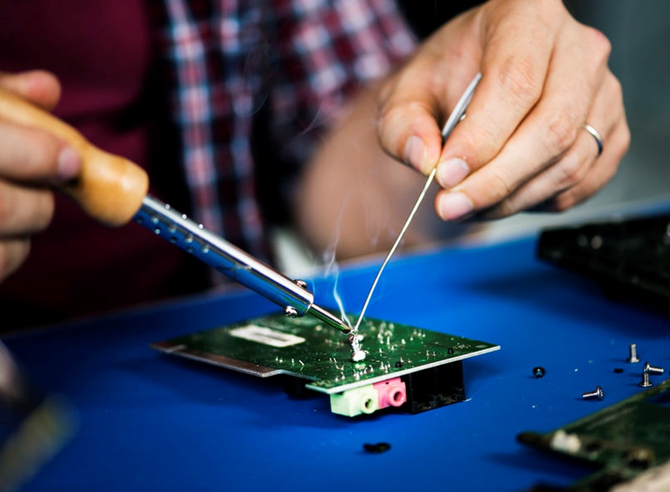
Comparative Analysis: Wave Soldering vs. Hand Soldering
The dichotomy between automation and manual craftsmanship is a central theme in process engineering. While automation suggests consistency, manual soldering offers agility. Determining "which is best" is rarely a binary choice but rather a function of the product lifecycle stage and complexity.
The Volume-Complexity Matrix
The industry standard approach to selecting between wave and hand soldering involves analyzing the Volume-Complexity Matrix:
Prototype and Low-Volume High-Mix (LVHM):
In the initial stages of New Product Introduction (NPI), setting up a wave soldering profile—which involves optimizing conveyor speed, wave height, and preheat dwell times—is often cost-prohibitive. Here, skilled technicians utilizing hand soldering stations offer the flexibility to assemble complex boards without the overhead of tooling and profile generation.
Mass Production:
As volumes scale into the thousands, the human variable becomes a liability regarding consistency and throughput. Wave soldering ensures that every joint receives identical thermal exposure, adhering to Six Sigma repeatability standards.
Thermal Profiling and Joint Consistency
A critical differentiator lies in thermal control. Wave soldering machines utilize closed-loop feedback systems to maintain solder pot temperatures within ±1°C. Conversely, hand soldering relies heavily on the operator's training and the thermal recovery speed of the soldering iron tip. While manual soldering allows for immediate visual inspection and adjustment, it lacks the simultaneous throughput of the wave process.
Unsure which methodology aligns with your current project scale? Review our comparative guide: Wave Soldering vs. Hand Soldering: Which Method is Best for Your Project?
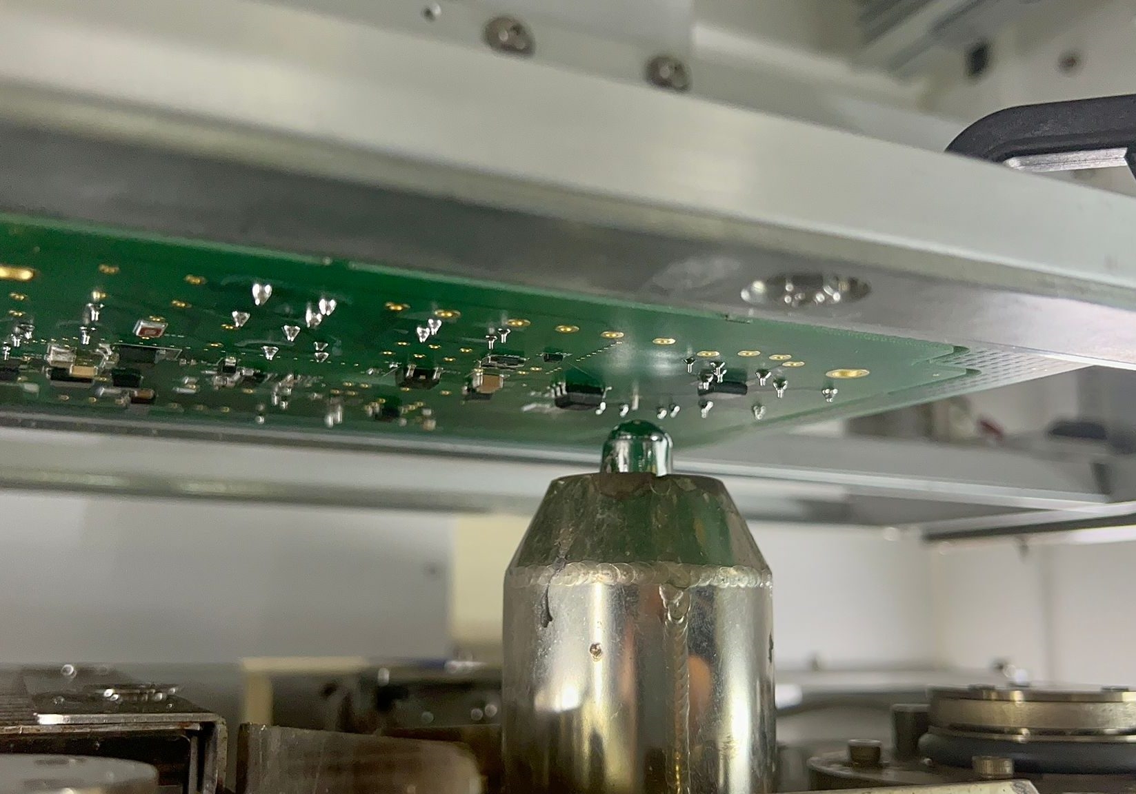
Selective Soldering: Bridging the Gap with Precision Automation
As PCB designs have evolved into mixed-technology boards—densely populated with both SMT components on the bottom side and THT components—traditional wave soldering has become problematic. The thermal stress of a wave can dislodge or damage SMT parts. Enter Selective Soldering, the precise middle ground between the brute force of wave soldering and the slowness of manual labor.
The Evolution of Robotic Precision
Selective soldering is arguably the most significant advancement in THT assembly for mixed-technology boards. Unlike wave soldering, which exposes the entire underside of the PCB to molten solder, selective soldering utilizes a miniature solder nozzle (often mounted on a 3-axis or greater robotic gantry) to target individual joints or rows of pins.
Process Capabilities and Flux Control
The selective process is defined by three programmable stages:
- Drop-Jet Fluxing: High-precision micro-dispensing of flux only onto the pads to be soldered. This eliminates the need for aggressive cleaning of flux residues across the entire board, a significant advantage for "No-Clean" processes.
- Active Preheating: Maintaining board temperature to facilitate wetting.
- Solder Nozzle Interaction: The nozzle approaches the board from beneath, soldering specific points without disturbing adjacent SMT components, often with clearances as tight as 1mm.
This method allows manufacturers to achieve the consistent quality of an automated process (meeting IPC Class 3 standards for high-reliability electronics) while accommodating the geometric complexities that would rule out wave soldering.
For a detailed look at how robotics are revolutionizing mixed-technology assembly, refer to : Achieving Precision in PCB Assembly: A Guide to Selective Soldering.
Manual Soldering in Harsh Environments: Techniques for Ruggedization
While automation dominates the factory floor, there are scenarios where manual soldering is not just an alternative, but a necessity—specifically in the realm of field repairs, oversized components, and high-reliability applications destined for harsh environments (e.g., aerospace, down-hole drilling, or automotive under-hood applications).
The Physics of Reliability Under Stress
Soldering for harsh environments requires a fundamental understanding of metallurgical fatigue and coefficient of thermal expansion (CTE) mismatches. A joint that passes a standard continuity test may fail catastrophically when subjected to:
- High-G Vibration: Causing work hardening and eventual cracking of the solder alloy.
- Thermal Cycling: Where rapid heating and cooling stress the intermetallic bond.
Specialized Techniques and Alloys
Technicians operating in this domain must employ advanced techniques that go beyond standard IPC-A-610 requirements. This includes:
- Mechanical Reinforcement: Utilizing hooks, wraps, and turret terminals to provide mechanical strength before the solder is applied.
- Alloy Selection: Moving beyond standard SAC305 (Sn-Ag-Cu) to high-temperature alloys or leaded equivalents (where RoHS exemptions apply) that offer superior ductility.
- Conformal Coating Preparation: Ensuring joints are meticulously cleaned of flux residues to prevent delamination of subsequent protective coatings.
Reliability in harsh environments is less about the speed of the joint formation and more about the wetting angle and the voiding percentage within the joint.
Learn about the specific techniques required to ensure connection integrity under extreme stress in our article: Manual Soldering in Harsh Environments: Techniques for Reliable Connections
Quality Assurance: Troubleshooting and Defect Mitigation
Regardless of whether the soldering method is wave, selective, or manual, the ultimate metric of success is the integrity of the solder joint. Defect analysis is a critical feedback loop in PCBA manufacturing. Adherence to industry standards, specifically IPC-A-610 (Acceptability of Electronic Assemblies), is the baseline for quality control.
Common Failure Modes and Root Cause Analysis
Troubleshooting is not merely fixing a defect; it is diagnosing the process drift that caused it. Common anomalies include:
Cold Solder Joints:
Characterized by a dull, grainy appearance and poor wetting.
Root Cause: Insufficient heat transfer, possibly due to a thermal profile that is too fast or an oxidized pad.
Solder Bridges (Shorts):
Unwanted connections between pads.
Root Cause: Often caused by excessive solder application, incorrect drag speed in wave soldering, or insufficient flux activity.
Tombstoning:
Where a passive component stands up on one end.
Root Cause: Uneven wetting forces during reflow, often due to thermal imbalances between pads.
The Diagnostic Approach
Effective troubleshooting requires a systematic approach involving visual inspection (AOI), X-ray analysis (for BGA and hidden joints), and cross-sectioning. Understanding the phase diagram of the solder alloy and the activation temperature of the flux is essential for tweaking the process parameters to eliminate these defects at the source.
Conclusion: Orchestrating the Perfect Assembly Process
The landscape of PCB soldering is dynamic, governed by the relentless pursuit of miniaturization and reliability. There is no single "correct" method; rather, there is an optimal method for every specific design and volume requirement.
- Wave Soldering remains the king of high-volume THT efficiency.
- Selective Soldering provides the necessary precision for modern mixed-technology boards.
- Manual Soldering offers indispensable agility for prototyping and ensuring reliability in the harshest environments.
Success in electronics manufacturing is achieved not by adhering rigidly to one method, but by understanding the scientific principles and industrial standards that underpin them all. By mastering these diverse methodologies and maintaining a rigorous focus on defect troubleshooting and quality assurance, manufacturers can ensure that their products meet the exacting standards of today's technology market.


