Introduction
High-frequency amplifiers demand precise PCB layouts to deliver clean signals and avoid oscillations. A 6-layer PCB provides the routing flexibility needed for RF paths while incorporating dedicated planes for power and ground. In 6-layer PCB RF amplifier design, engineers balance trace widths, via placement, and layer stacking to maintain integrity up to several gigahertz. This setup supports applications in wireless communication and radar systems.
From an assembly perspective, poor design leads to yield drops during soldering and testing. I've encountered boards where unmatched impedances caused reflections, spiking return loss beyond acceptable levels. Optimizing performance involves targeted techniques for impedance control and noise suppression. Stability analysis ensures the amplifier operates without unintended feedback loops. This article draws on hands-on experience to outline practical steps. Key focus areas include 6-layer PCB impedance matching, grounding strategies, isolation methods, and analysis tools. Follow these to enhance reliability in your RF projects.
What Is 6-Layer PCB Design for High-Frequency Amplifiers and Why It Matters
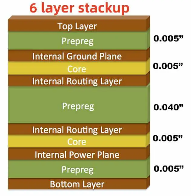
6 layers PCB design for high-frequency amplifiers refers to the structured layout of conductive and dielectric layers tailored for RF signal amplification. It typically features outer signal layers, inner power and ground planes, and additional routing layers for control signals. This configuration isolates sensitive RF paths from digital noise, enabling gains in the 1-10 GHz range.
These designs matter in performance-critical systems. Amplifiers in base stations or test equipment require low phase noise and high linearity. Without proper layering, parasitic inductances degrade output power. Assembly challenges arise when vias introduce discontinuities, leading to rework. In production, stable designs reduce test failures by ensuring consistent S-parameters.
Experience shows that 6-layer boards not only reduce the circuit board cost but also ensure quality over higher counts for mid-range frequencies. They comply with IPC-2221B guidelines for multilayer routing. For RF, adherence to IPC-2228 ensures microwave-grade integrity. Procurement teams specify these for projects needing robust thermal handling during high-power operation.
Technical Principles in 6-Layer PCB RF Amplifier Design
RF amplifier design hinges on electromagnetic principles to preserve signal fidelity. At high frequencies, skin effect confines currents to trace surfaces, demanding wider conductors. Dielectric losses in laminates attenuate signals, so low-loss materials per IPC-4101E become essential.
6-Layer PCB Impedance Matching Fundamentals
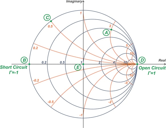
Impedance matching prevents reflections that distort waveforms. In a 6-layer stackup, characteristic impedance depends on trace width, height to reference plane, and dielectric constant. IPC-2141A provides equations for microstrip and stripline calculations, targeting 50 ohms for RF inputs.
Designers model traces using field solvers to account for fringing fields. Mismatches at junctions, like amplifier inputs, create standing waves. Practical tip: Taper transitions gradually to broadband match. Assembly verification involves time-domain reflectometry to spot discontinuities early.
6-Layer PCB Grounding for RF Integrity
Grounding for RF establishes low-impedance return paths to minimize loop areas. Dedicated ground planes in layers 2 and 5 shield signals and provide stitching vias. IPC-2228 recommends plane splits only where necessary, with fences to contain fields.
Poor grounding invites common-mode currents, coupling noise into amplifiers. In multilayer boards, via fences around RF sections form virtual walls. Experience highlights the need for symmetric stitching to avoid current crowding at edges.
6-Layer PCB Isolation Techniques
Isolation techniques separate RF from DC or digital sections to curb crosstalk. Guard traces or moats in ground planes block leakage. IPC-2221B specifies minimum spacing based on frequency, often 3 times the substrate height for 1 dB isolation.
In 6-layer designs, inner layers dedicate to RF isolation. Faraday cages via enclosures add external shielding. During assembly, I've troubleshot boards where insufficient isolation caused intermodulation distortion, resolved by adding grounded coplanar waveguides.
6-Layer PCB Stability Analysis Basics
Stability analysis assesses feedback risks in amplifiers. It involves calculating gain margins and phase shifts across frequencies. Tools simulate S-parameters to predict oscillations per IPC-2228 microwave guidelines.
Key metrics include K-factor for unconditional stability. Unstable designs exhibit negative resistance at outputs. Layering aids by shortening feedback paths. Practical checks confirm roll-off in gain beyond bandwidth.
Practical Solutions and Best Practices for Optimization
Implement these steps to optimize 6-layer RF amplifier boards. Start with stackup planning: Position RF signals adjacent to ground planes for tight coupling. Use 0.8 mm dielectric thickness for 50-ohm lines, per IPC-2141A formulas.
For 6-layer PCB impedance matching, employ edge-coupled lines for balanced outputs. Simulate with 3D solvers to refine widths. Fabricate test coupons on panels for validation.
In 6-layer PCB grounding for RF, place vias every lambda/20 along traces. Connect planes with dense arrays to form solid returns. Avoid slots under signal paths.
Apply 6-layer PCB isolation techniques by routing RF on top layers and controls on bottom. Use grounded vias as barriers, spaced at quarter-wavelength intervals.
Conduct 6-layer PCB stability analysis iteratively. Prototype with tunable components to measure margins. Adjust bias networks for optimal negative feedback.
Assembly best practices include low-residue fluxes to prevent residue-induced shorts. Bake boards pre-reflow to eliminate moisture per JEDEC J-STD-020E.
Troubleshooting Insights from Assembly Experience
In assembly lines, RF boards often fail stability tests due to overlooked vias. One case involved a 6-layer amplifier oscillating at 2.4 GHz. Root cause: Unstitched ground plane allowed slotline modes. Solution: Added 20 vias per inch, dropping noise floor by 15 dB.
Another issue: Isolation failures from via stub resonances. Trimming stubs post-drill resolved it, but redesign with blind vias prevented recurrence. For impedance drifts, thermal cycling exposed CTE mismatches; switching to low-alpha laminates stabilized traces.
Experience-based advice: Always cross-section prototypes per IPC-TM-650 2.1.1 to inspect layer alignment. These fixes boost yields from 70% to over 95% in RF runs.
Suggested Reading: 6-Layer PCB Assembly Demystified: Best Practices for Reliable Manufacturing
Conclusion
6-layer PCB design for high-frequency amplifiers thrives on precise impedance, grounding, isolation, and stability measures. These elements ensure optimal performance in demanding RF environments. Hands-on practices from assembly refine theoretical plans into reliable products.
Adopt IPC-guided techniques to sidestep common pitfalls. Regular analysis and prototyping build confidence in designs. For your next amplifier project, prioritize layered integrity to achieve stable, high-gain outputs.
FAQs
Q1: How does 6-layer PCB impedance matching improve RF amplifier performance?
A1: 6-layer PCB impedance matching minimizes reflections for cleaner signal transfer in amplifiers. Use stripline configurations with ground planes to hit 50 ohms precisely. In assembly, verify with VNA sweeps to catch mismatches early. This boosts return loss and prevents gain ripple across bands.
Q2: What are effective 6-layer PCB grounding for RF techniques to reduce noise?
A2: Effective 6-layer PCB grounding for RF involves full planes and via stitching to shorten return paths. Fence vias around active areas block EMI. From experience, dense grids cut common-mode coupling. Follow IPC-2228 for plane integrity to maintain low phase noise in amplifiers.
Q3: Why implement 6-layer PCB isolation techniques in high-frequency designs?
A3: 6-layer PCB isolation techniques prevent crosstalk between RF and digital sections. Moats and guard traces provide 20 dB separation. Assembly troubleshooting shows they avoid distortion in multi-function boards. IPC-2221B spacing rules ensure compliance for stable operation.
Q4: How to perform 6-layer PCB stability analysis during design validation?
A4: Perform 6-layer PCB stability analysis by simulating K-factors and rolling off excess gain. Prototype tests measure phase margins under load. Experience reveals bias tweaks often fix marginal stability. Use IPC-2228 guidelines for microwave validation to avoid field oscillations.
IPC-2221B — Generic Standard on Printed Board Design. IPC, 2009.
IPC-2228 — Sectional Design Standard for High Frequency (RF)/Microwave Printed Boards and Assemblies. IPC, 2022.
IPC-2141A — Design Guide for High-Speed Controlled Impedance Printed Boards. IPC, 2006.
IPC-4101E — Specification for Base Materials for Rigid and Multilayer Printed Boards. IPC, 2010.
IPC-TM-650 — Test Methods Manual. IPC, various revisions.
JEDEC J-STD-020E — Moisture/Reflow Sensitivity Classification. JEDEC, 2014.


