Introduction
In high-density interconnect (HDI) PCB design, blind vias and buried vias play a critical role in achieving compact layouts and efficient signal routing. These vias allow connections between specific layers without penetrating the entire board thickness, freeing up surface area for components and traces. Engineers rely on them to meet the demands of modern electronics, where smaller form factors and higher interconnect densities are essential. Understanding their implementation ensures reliable performance in applications requiring advanced packaging. This article explores the fundamentals, manufacturing processes, and best practices for blind vias and buried vias in HDI PCB design.
What Are Blind Vias and Buried Vias and Why Do They Matter in HDI PCB Design?
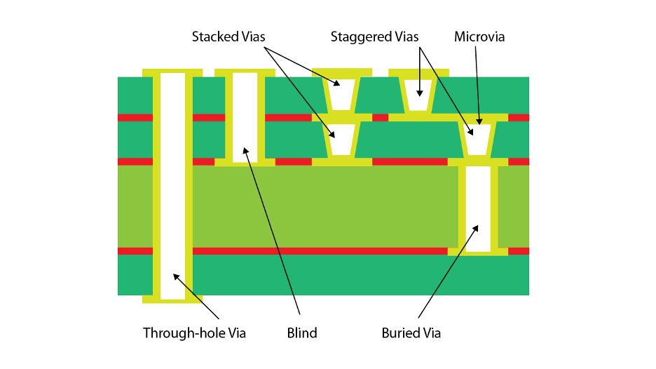
Blind vias connect an outer layer to one or more inner layers but stop short of reaching the opposite side of the board. Buried vias, in contrast, link only inner layers, remaining completely hidden from the surface. Both differ from standard through vias, which span the full board thickness and consume valuable real estate on outer layers. In HDI PCB design, these vias enable finer pitch components, such as ball grid arrays, by minimizing via stubs that cause signal integrity issues. They support higher layer counts and routing density, making them indispensable for devices with stringent size constraints.
The relevance of blind vias and buried vias stems from the evolution of electronics toward miniaturization. Traditional multilayer boards with through vias limit density due to fanout requirements around large pads. By using blind vias and buried vias, designers reduce layer transitions and shorten signal paths, improving electrical performance. This approach aligns with the needs of electric engineers working on high-speed circuits, where impedance control and crosstalk reduction are paramount. As board complexity increases, these vias become key to balancing manufacturability and functionality.
Related Reading: Unlocking PCB Density: A Beginner's Guide to Blind Vias
Technical Principles of Blind and Buried Vias
The core principle behind blind vias and buried vias lies in their selective layer connectivity, achieved through precise drilling and plating techniques. Blind vias typically start from the top or bottom layer and terminate at a specific inner layer, often created using laser ablation for microvia sizes. Buried vias require drilling through specific inner cores before lamination, ensuring no exposure to outer surfaces. Both types demand careful control of hole geometry to facilitate uniform copper plating, which is vital for conductivity and thermal dissipation.
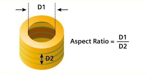
Via aspect ratio, defined as the ratio of via depth to diameter, governs the feasibility of plating and reliability. A well-managed via aspect ratio prevents voids or thinning in the copper barrel, which could lead to open circuits under thermal stress. In HDI PCB design, laser-drilled blind vias often feature shallower depths compared to mechanical drills, allowing tighter aspect ratios. Engineers must consider material properties, such as dielectric thickness, to optimize this parameter during stackup planning.
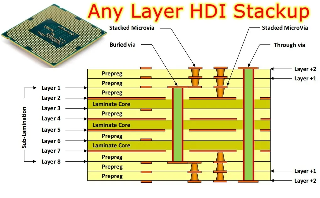
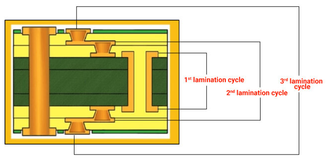
Sequential lamination forms the backbone of manufacturing boards with blind vias and buried vias. This process involves building the stackup in stages: first laminating inner cores with buried vias, then adding outer layers with blind vias through additional buildup cycles. Each cycle includes via formation, plating, and dielectric application, allowing for stacked or staggered via configurations. This method accommodates complex HDI structures, such as Type II or Type III, where multiple blind via layers interconnect.
Reliability hinges on factors like plating thickness uniformity and intermetallic formation during assembly. Blind vias reduce stub inductance, enhancing high-frequency signal integrity, while buried vias preserve outer layer integrity for fine-pitch routing. Adhering to standards like IPC-2226A ensures these principles translate into robust designs.
Related Reading: Blind Vias in PCB Design: Optimizing High-Density Boards
Manufacturing Processes for Blind and Buried Vias in HDI PCBs
Fabricating blind vias and buried vias requires specialized processes tailored to HDI PCB design. Buried vias are drilled mechanically into inner core panels before initial lamination, followed by electroless and electrolytic plating to metallize the holes. Blind vias, often microvias, use UV or CO2 lasers to ablate dielectric material precisely, exposing inner copper pads without damaging deeper layers. Post-drilling, sequential plating fills or plates the vias, sometimes with conductive or non-conductive fills for planarization.
Sequential lamination cycles repeat for advanced HDI builds, enabling stacked blind vias where one via lands on another’s pad. Each lamination step bonds prepreg or resin-coated copper (RCC) to the existing stack, followed by via drilling and metallization. Controlling via aspect ratio during these steps prevents plating defects, such as dog-boning or overplating. Thermal expansion mismatches between copper and dielectric must be managed to avoid via cracking during reflow.
Inspection verifies via quality through cross-sectioning, electrical testing, and X-ray analysis. Standards such as IPC-6016 provide qualification criteria for HDI features, including via pull strength and continuity. These processes demand precise registration to align vias across layers, especially in high-layer-count boards.
Best Practices for Implementing Blind and Buried Vias
Engineers should plan stackups early, grouping signals to minimize buried via usage in high-speed nets. Symmetrical builds with blind vias on both sides reduce warpage risks during lamination. Maintain conservative via aspect ratios by selecting thinner dielectrics for blind vias, balancing density with manufacturability. Staggered vias, where blind vias do not stack directly, distribute stress better than filled stacked configurations.
In HDI PCB design, allocate escape routing for blind via fans under BGA pads, using microvias for direct component connection. Simulate thermal and mechanical stresses to predict via reliability under cycling conditions. Follow IPC-2221B guidelines for pad sizing and annular ring dimensions to prevent drill breakout.
Document via types clearly in fabrication drawings, specifying drill methods and fill options. Collaborate with fabricators on capabilities, such as laser types and lamination presses, to refine designs. These practices enhance yield and performance.
Troubleshooting Common Issues with Blind and Buried Vias
Via opens often trace back to excessive via aspect ratios causing plating voids. Cross-section analysis reveals barrel cracks from CTE mismatch in sequential lamination. Engineers can mitigate by selecting low-CTE materials and verifying plating thickness uniformity.
Signal integrity problems arise from unterminated blind via stubs resonating at high frequencies. Shortening stubs or filling vias resolves this. Warpage in asymmetric HDI builds stresses buried vias; balanced stackups and controlled curing prevent failures.
Conclusion
Blind vias and buried vias enable the high interconnect density essential to HDI PCB design. Their strategic use, guided by via aspect ratio control and sequential lamination, optimizes space and performance. Engineers benefit from structured planning and adherence to industry standards for successful implementation. Mastering these elements unlocks compact, reliable boards for demanding applications.
FAQs
Q1: What are the differences between blind vias and buried vias in HDI PCB design?
A1: Blind vias connect an outer layer to inner layers without traversing the full board, while buried vias interconnect only inner layers. Both enhance routing density but require distinct manufacturing steps like laser drilling for blind vias and core drilling for buried. Proper stackup planning ensures alignment and reliability in HDI PCB design.
Q2: Why is via aspect ratio important for blind vias and buried vias?
A2: Via aspect ratio, the depth-to-diameter ratio, affects plating quality and current-carrying capacity. High ratios lead to plating defects in blind vias and buried vias, compromising reliability. In HDI PCB design, keeping ratios low supports uniform copper deposition during sequential lamination cycles.
Q3: What role does sequential lamination play in HDI PCB design with blind and buried vias?
A3: Sequential lamination builds HDI PCBs layer by layer, incorporating buried vias in cores and blind vias in outer buildups. This process allows stacked or staggered configurations for complex routing. It demands precise control to maintain via aspect ratio and registration across cycles.
Q4: How do blind vias and buried vias improve HDI PCB performance?
A4: They reduce via stubs, minimizing inductance and improving signal integrity at high speeds. Surface space savings enable finer traces and component placement. Combined with sequential lamination, they achieve higher densities without sacrificing reliability.
References
IPC-2221B — Generic Standard on Printed Board Design. IPC
IPC-2226A — Sectional Design Standard for High Density Interconnect (HDI) Printed Boards. IPC
IPC-6016 — Qualification and Performance Specification for High Density Interconnect (HDI) Printed Boards. IPC


