Introduction
Blind vias play a critical role in modern printed circuit board designs where space constraints demand higher interconnect density without compromising reliability. In industries such as aerospace, medical, and automotive, high reliability blind via structures ensure signal integrity and mechanical stability under extreme conditions. These vias connect surface layers to inner layers without penetrating the full board thickness, enabling compact multilayer stackups. Designers must adhere to rigorous standards to mitigate risks like via cracking or delamination during thermal cycling. This article explores the engineering principles, best practices, and standard compliance essential for high reliability blind via implementation.
Engineers targeting aerospace PCB design face unique challenges from vibration and temperature extremes, while medical PCB design prioritizes biocompatibility and long-term stability. Automotive PCB design adds requirements for thermal shock resistance and electromagnetic compatibility. IPC standards blind via specifications provide the framework for qualification across these sectors. By understanding these elements, designers can achieve robust performance that meets stringent industry demands.
What Are Blind Vias and Why Do They Matter in High-Reliability Applications?
Blind vias are vertical interconnects that link an outer layer to one or more internal layers, stopping short of the opposite side of the board. Unlike through-hole vias, they free up inner layer routing space, which is vital for high-density interconnects in complex assemblies. In high reliability blind via designs, these structures must withstand operational stresses without failure, as downtime in critical systems can have severe consequences. For instance, in aerospace PCB design, blind vias support compact avionics where weight and size are paramount.
The relevance stems from the push for miniaturization coupled with elevated performance needs. Medical PCB design benefits from blind vias in implantable devices requiring minimal profiles and reliable signal paths. Automotive PCB design leverages them for advanced driver-assistance systems under harsh thermal and vibrational loads. However, improper design can lead to reliability issues like barrel cracking or plating voids, underscoring the need for precise engineering.
Adherence to IPC standards blind via guidelines ensures consistency in fabrication and inspection. These standards define acceptability criteria for plating uniformity and structural integrity. Engineers must balance density gains with risk mitigation to deliver boards that perform over extended lifecycles.
Related Reading: Unlocking PCB Density: A Beginner's Guide to Blind Vias
Technical Principles of High-Reliability Blind Via Formation
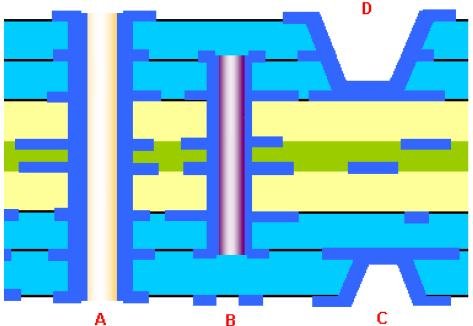
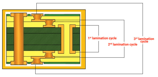
Blind vias are typically formed through sequential lamination processes, where core sections are built incrementally to expose specific layer pairs for drilling. Mechanical drilling or laser ablation creates the hole, followed by electroless copper deposition and electroplating to form the conductive barrel. The aspect ratio, defined as depth to diameter, must be controlled to prevent plating defects that compromise reliability. In high reliability blind via applications, thermal mismatch between copper plating and dielectric materials induces stress during reflow or operation.
Plating quality is paramount, as thin or uneven copper leads to electromigration or void formation under current. IPC-6012 outlines performance requirements for rigid boards, including via plating thickness and adhesion for Class 3 products used in high-reliability sectors. Cross-section analysis reveals common failure modes like corner cracking in laser-drilled vias due to heat-affected zones. Engineers mitigate these by selecting resins with matched coefficients of thermal expansion.
Reliability testing simulates field conditions through thermal cycling, where blind vias endure expansion and contraction cycles. Vibration testing, critical for automotive PCB design, assesses mechanical integrity. These principles guide stackup planning to distribute via stresses evenly across layers.
Related Reading: Blind Vias in PCB Design: Optimizing High-Density Boards
Design Challenges and Failure Mechanisms in Stringent Environments
High reliability blind via structures face amplified challenges in aerospace, medical, and automotive environments. Temperature fluctuations cause differential expansion, stressing the via-plated interface and potentially causing separation. Humidity ingress exacerbates corrosion in uncapped vias, particularly in medical PCB design where sterilization cycles are routine. Vibration in automotive applications induces fatigue, leading to microcracks that propagate over time.
IPC standards blind via criteria, such as those in Class 3, demand zero tolerance for certain defects like knitline separation in plating. Sequential build-up increases warpage risk if core alignment falters during lamination. Signal integrity degrades if blind via stubs act as impedance discontinuities in high-speed circuits. Designers must model these effects using finite element analysis to predict long-term behavior.
Fabrication variables like drill smear removal and desmear processes directly impact void-free plating. Inadequate cleaning leaves resin residues that hinder copper adhesion, accelerating failure.
Practical Best Practices for High-Reliability Blind Via Implementation
Start with stackup optimization, positioning blind vias in low-stress regions and staggering them to avoid clustering. Select high-Tg laminates for better dimensional stability under thermal loads. Maintain conservative aspect ratios to ensure uniform plating, as recommended in IPC guidelines. For aerospace PCB design, incorporate via-in-pad configurations with non-conductive fills to enhance planarization and reliability.
Specify capped vias where planar surfaces are needed, preventing solder wicking during assembly. Collaborate early with fabricators for design for manufacturability reviews, confirming sequential lamination feasibility. Implement via protection schemes like filled or tented vias per IPC-4761 to shield against contaminants.
Inspection protocols include electrical continuity testing, X-ray for barrel quality, and microsectioning for plating integrity. In medical PCB design, biocompatibility testing verifies no leachables from via materials. Automotive PCB design requires accelerated life testing to validate under hood conditions.
Use simulation tools to verify thermal performance before prototyping. Document deviations from standard via types, ensuring traceability.
Troubleshooting Common Blind Via Reliability Issues
Engineers often encounter via opens after thermal shock, traced to plating cracks from high aspect ratios. Solution involves redesigning with staggered vias and verified plating processes. Delamination at the via pad signals poor adhesion; review desmear and plasma treatment efficacy.
Warpage post-lamination affects blind via alignment, mitigated by symmetric stackups and controlled cure cycles. In aerospace PCB design, outgassing during vacuum exposure indicates trapped volatiles; bake-out panels prior to assembly. For medical applications, ionic contamination testing isolates via-related failures.
Systematic root cause analysis using failure mode effects aligns with IPC Class 3 verification.
Conclusion
High reliability blind via design demands a holistic approach integrating material selection, process control, and standard compliance. Aerospace, medical, and automotive sectors rely on these vias for density and performance, but only when engineered against failure modes. IPC standards provide the benchmark for qualification, ensuring boards meet Class 3 rigor. By following structured best practices, engineers deliver PCBs that excel in demanding environments. Future advancements in laser drilling and plating will further enhance capabilities.
FAQs
Q1: What makes high reliability blind via critical for aerospace PCB design?
A1: High reliability blind via structures enable compact avionics layouts while withstanding vibration, thermal extremes, and radiation. IPC standards blind via requirements ensure plating integrity and zero defects in Class 3 boards. Proper stackup and sequential lamination prevent cracking during flight cycles. This approach maintains signal reliability in mission-critical systems.
Q2: How do IPC standards blind via guidelines apply to medical PCB design?
A2: IPC standards blind via specifications in IPC-6012 Class 3 dictate uniform plating and adhesion for long-term stability. Blind vias support dense interconnects in devices like pacemakers without risking failure from body fluids or sterilization. Engineers prioritize filled vias to eliminate crevices. Compliance verifies biocompatibility and reliability over implant lifespans.
Q3: Why choose blind vias in automotive PCB design for high reliability?
A3: Blind vias optimize space in engine control units exposed to heat and shock, reducing inductance compared to through vias. High reliability blind via practices include conservative aspect ratios and robust plating per IPC guidelines. They enhance thermal management by freeing inner layers. Testing under automotive conditions confirms durability.
Q4: What are key best practices for implementing high reliability blind via?
A4: Optimize stackups for stress distribution and use sequential processes for precise depth control. Adhere to IPC Class 3 for plating and inspection. Employ fills or caps for protection, and simulate thermal-mechanical performance. Early DFM collaboration avoids manufacturability pitfalls.
References
IPC-6012F — Qualification and Performance Specification for Rigid Printed Boards. IPC, 2023
IPC-6012DS — Qualification and Performance Specification for Rigid Printed Boards for Avionics Hardware. IPC, 2023
IPC-2221B — Generic Standard on Printed Board Design. IPC, 2012
IPC-A-600K — Acceptability of Printed Boards. IPC, 2020


