Introduction
In modern PCB design, achieving optimal signal integrity demands precise control over electrical characteristics. Impedance matching ensures that signals propagate without distortion across high-speed interfaces. As data rates climb into gigabits per second, mismatches lead to reflections, crosstalk, and bit errors. Electric engineers must master PCB impedance matching to meet performance targets in applications like telecommunications and computing. This article explores the principles, techniques, and best practices for effective impedance control. By understanding these elements, designers can enhance reliability and reduce development iterations.
What Is Impedance Matching and Why It Matters
Impedance matching in PCBs refers to designing traces and structures so their characteristic impedance aligns with the source and load impedances. Characteristic impedance arises from the transmission line properties of PCB traces, modeled as distributed inductors and capacitors. When matched, maximum power transfers without reflection. Signal reflection from impedance mismatch causes ringing, overshoot, and attenuation, degrading signal integrity.
The relevance grows with rising edge speeds in digital signals. Faster transitions shorten the rise time, making traces behave as transmission lines even at moderate lengths. Uncontrolled impedance amplifies these effects, leading to timing skew and electromagnetic interference. Compliance with standards like IPC-2221 ensures consistent performance across manufacturing variations. Engineers prioritize impedance control techniques to maintain eye diagram quality and meet timing budgets. Ultimately, proper matching supports higher data rates and smaller form factors.

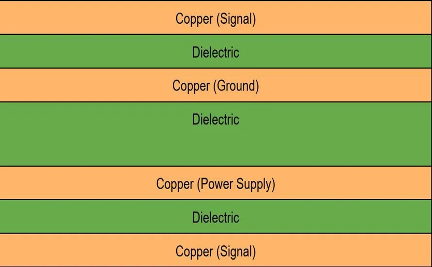
Technical Principles of PCB Impedance
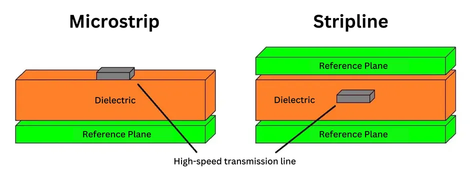
The foundation of PCB impedance matching lies in transmission line theory. The characteristic impedance Z0 of a trace equals the square root of inductance per unit length divided by capacitance per unit length. For microstrip lines, exposed on one side to air, Z0 depends on trace width, copper thickness, substrate height, and dielectric constant. Striplines, embedded between planes, offer more stable impedance due to symmetric fields but require careful spacing.
Dielectric materials influence capacitance directly through their relative permittivity, typically 3.5 to 4.5 for common FR-4. Variations in glass weave or resin content cause local impedance fluctuations. Conductor geometry, including etch tolerances, further modulates Z0. Engineers calculate these using field solver approximations or empirical formulas from IPC-2141. Frequency dependence emerges at gigahertz ranges, where skin effect increases effective resistance. Understanding these interactions prevents surprises in prototypes.
Differential pairs introduce coupled impedance, where even and odd mode velocities must balance. Common mode impedance affects noise rejection, while differential drives data transmission. Length matching within tolerances, often 5 mils, preserves phase alignment. Vias and bends disrupt uniformity, introducing discontinuities equivalent to capacitive or inductive loads. Modeling these ensures predictions match measurements.
Factors Influencing Impedance Control
Several stackup parameters dictate achievable impedance. Reference plane proximity sets capacitance; closer planes lower Z0. Prepreg and core thicknesses, along with their dielectric constants, require balancing for multilayer boards. Trace routing over splits or plane voids raises loop inductance, deviating Z0.
Manufacturing tolerances impact final values. Etch variation of 20% alters width significantly, shifting impedance by several ohms. Material properties vary batch-to-batch, demanding statistical process control. IPC-6012 specifies qualification for performance classes, including impedance verification methods. Engineers specify tolerances like ±10% for single-ended 50-ohm lines or ±5% for high-speed.
Environmental factors, such as temperature and humidity, subtly affect dielectrics. Coefficient of thermal expansion mismatches cause warpage, stressing traces. Frequency-dependent losses from conductor roughness and dielectric absorption degrade signals over distance.
Practical Solutions and Best Practices for Impedance Matching
Designers start with stackup planning to support target impedances. Symmetric builds with dedicated power and ground planes provide return paths, minimizing loop area. For 50-ohm single-ended traces, typical widths range from 4 to 7 mils on 1.6mm boards, adjusted via iteration.
Impedance matching calculators simplify geometry determination. These tools input stackup details, including layer thicknesses, Er, and copper weights, outputting width and spacing. Users verify with time-domain reflectometry (TDR) simulations. Allocate margins for fab tolerances, aiming for center values.
Routing strategies enhance control. Avoid 90-degree bends; use 45-degree or curved paths to reduce reflections. Length-tune differential pairs post-layout. Place vias symmetrically for transitions, adding stubs if needed for compensation. Ground stitching vias around splits maintain reference integrity.
Testing confirms design. TDR measurements quantify Z0 along traces, identifying discontinuities. Vector network analyzers assess insertion and return loss. Correlate simulations to measurements, refining models. For production, specify impedance on fab drawings with net classes.
Common Challenges and Troubleshooting
Impedance mismatches often stem from incomplete stackup specs. Engineers overlook prepreg flow, compressing layers and altering heights. Solution involves vendor collaboration on material datasheets and coupon testing.
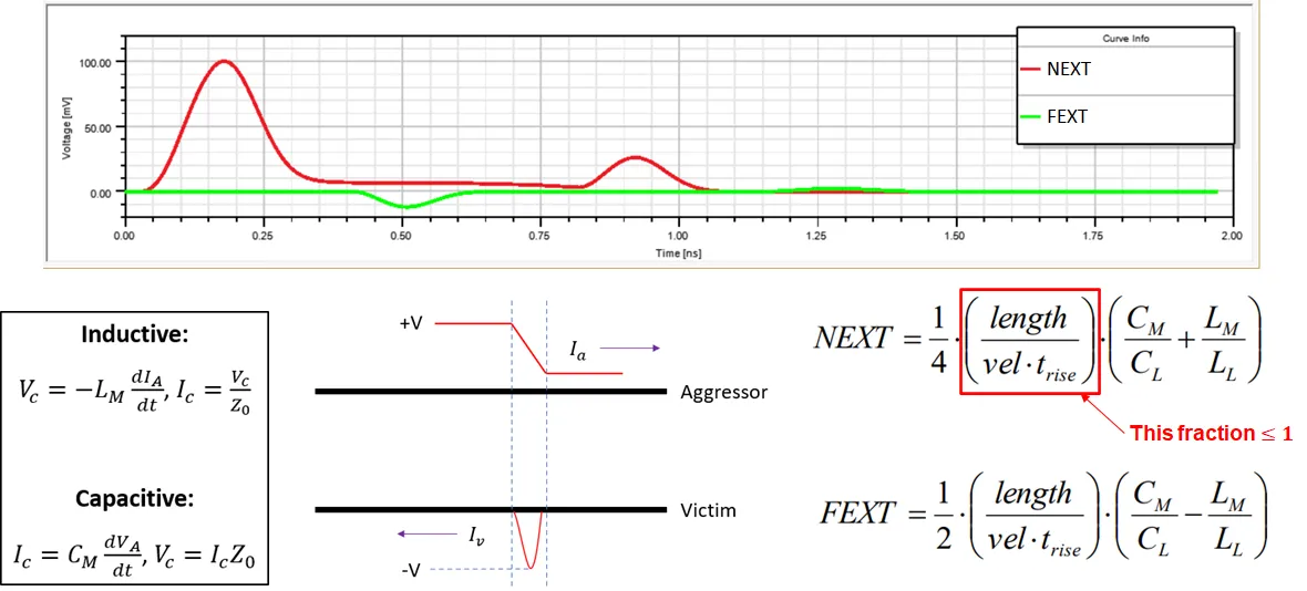
Crosstalk from adjacent aggressor traces couples noise. Increase spacing per coupling rules, or shield with grounded traces. Via stubs resonate at quarter-wave frequencies; back-drill or use blind vias to shorten.
High-density designs crowd planes, creating impedance gradients. Segment planes carefully, ensuring overlap under signals. Differential skew from unequal etch rates requires serpentine meanders for tuning.
Post-assembly, connectors introduce mismatches. Match PCB Z0 to cable specs, using series resistors if needed. Systematic debugging with oscilloscopes pinpoints issues.
Conclusion
Mastering PCB impedance matching unlocks reliable high-speed performance. From transmission line fundamentals to stackup optimization, each step contributes to signal integrity. Implementing impedance control techniques, supported by calculators and standards like IPC-2221, IPC-2141, and IPC-6012, minimizes reflections and ensures consistency. Engineers benefit from proactive design, verification, and troubleshooting. Prioritizing these practices reduces risks and accelerates time-to-market.
FAQs
Q1: What are the main impedance control techniques for PCB impedance matching?
A1: Impedance control techniques include precise trace width and spacing adjustments based on stackup parameters. Designers use symmetric reference planes and dielectric selection to achieve target Z0. Verification via TDR ensures tolerances like ±10%. These methods prevent signal reflection impedance mismatch in high-speed designs. Consistent application aligns with engineering best practices.
Q2: How does signal reflection from impedance mismatch affect PCB performance?
A2: Signal reflection impedance mismatch causes voltage overshoot, ringing, and eye closure in high-speed signals. Reflections bounce back, interfering with subsequent bits and increasing bit error rates. This degrades timing margins and EMI compliance. Proper PCB impedance matching eliminates these by ensuring continuous Z0. Engineers model and test to quantify impacts early.
Q3: What factors does an impedance matching calculator consider in PCB design?
A3: An impedance matching calculator evaluates trace width, thickness, dielectric constant, and layer height. It accounts for copper weight and reference plane proximity to compute Z0 for microstrip or stripline. Users input stackup details for accurate predictions. This tool aids impedance control techniques, reducing trial-and-error in layouts.
Q4: Why is stackup design critical for PCB impedance matching?
A4: Stackup design defines dielectric thicknesses and plane arrangements, directly influencing capacitance and inductance. Symmetric builds stabilize Z0 across frequencies. Poor planning leads to variations from fab tolerances. Engineers optimize for both impedance and thermal management. This foundation supports reliable signal integrity in multilayer boards.
References
IPC-2221 — Generic Standard on Printed Board Design. IPC
IPC-2141 — Design Guide for High-Density Interconnect (HDI) and Embedded Component PCBs. IPC
IPC-6012E — Qualification and Performance Specification for Rigid Printed Boards. IPC