Introduction
In modern printed circuit board (PCB) designs, especially those operating at high speeds, routing techniques play a critical role in preserving signal integrity. Electric engineers face increasing challenges as signal frequencies push into the gigahertz range, where even minor routing errors can lead to reflections, crosstalk, and electromagnetic interference (EMI). Proper implementation of differential pair routing, impedance controlled routing, avoiding vias in high-speed traces, minimizing trace length, and ground plane routing ensures data transmission remains accurate and reliable. These methods address fundamental transmission line behaviors, helping designs meet performance requirements without costly revisions. This article provides structured guidance on these techniques, drawing from established engineering principles to help engineers optimize their layouts systematically.
Signal integrity issues often manifest as bit errors, jitter, or complete signal failure in high-speed interfaces like those in telecommunications or computing systems. By focusing on controlled environments for signal propagation, engineers can predict and mitigate distortions early in the design phase. The following sections break down the technical foundations and practical applications of key routing strategies.
Why Signal Integrity Matters in PCB Routing
Signal integrity refers to the preservation of electrical signal quality throughout its propagation across the PCB. In high-speed designs, signals behave as transmission lines where mismatches in impedance or path discontinuities cause reflections that degrade waveform quality. Electric engineers must prioritize routing to minimize these effects, as poor signal integrity leads to timing skew, increased bit error rates, and system instability. Industry standards like IPC-2221 outline general design guidelines that emphasize consistent trace geometries and reference planes to support reliable signal transmission.
The relevance extends beyond performance to compliance and manufacturability. Designs ignoring these principles often fail electromagnetic compatibility (EMC) testing or require expensive respins. For instance, in multilayer boards, improper routing can couple noise between layers, amplifying issues in dense layouts. Understanding these implications allows engineers to integrate routing strategies from the schematic stage onward.
Core Principles of Transmission Line Theory in PCB Routing
Transmission line theory forms the backbone of effective PCB routing. Every trace acts as a distributed capacitor and inductor, characterized by its impedance, which depends on width, thickness, spacing, and surrounding dielectric. Reflections occur when the load impedance differs from the trace's characteristic impedance, quantified by the reflection coefficient formula. Engineers calculate these parameters using stackup details to predict behavior accurately.
Propagation delay, another key factor, arises from the signal's velocity in the medium, typically half the speed of light in FR-4 material. Length mismatches introduce skew, particularly problematic in clock or data lines. Return currents flow through the nearest ground plane, making its continuity essential for low-inductance paths. These principles guide all advanced routing techniques discussed here.
Crosstalk, both capacitive and inductive, increases with proximity and length of parallel traces. Shielding via ground planes or guard traces mitigates this by providing low-impedance return paths. By aligning routing with these mechanisms, engineers achieve predictable signal behavior across frequencies.
Mastering Differential Pair Routing
Differential pair routing transmits signals across two closely coupled traces carrying equal but opposite polarities. This configuration rejects common-mode noise, improving signal-to-noise ratio in high-speed applications. Engineers maintain tight coupling by keeping intra-pair spacing constant, typically 4 to 6 times the trace width, while ensuring the pair-to-pair spacing exceeds 5 times the intra-pair gap to minimize crosstalk.
Length matching within 5 mils or less prevents skew, achieved through serpentine patterns if needed. Reference both traces to the same ground plane to equalize propagation delays. Avoid sharp bends; use 45-degree or curved transitions to preserve impedance.
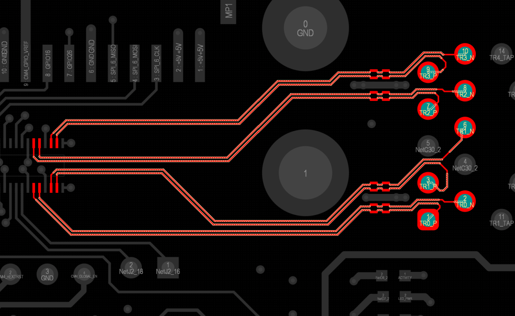
In practice, route pairs orthogonally to adjacent signals to reduce coupling. Symmetry in vias, if unavoidable, maintains balance. These steps ensure robust performance in interfaces requiring precise timing.
Implementing Impedance Controlled Routing
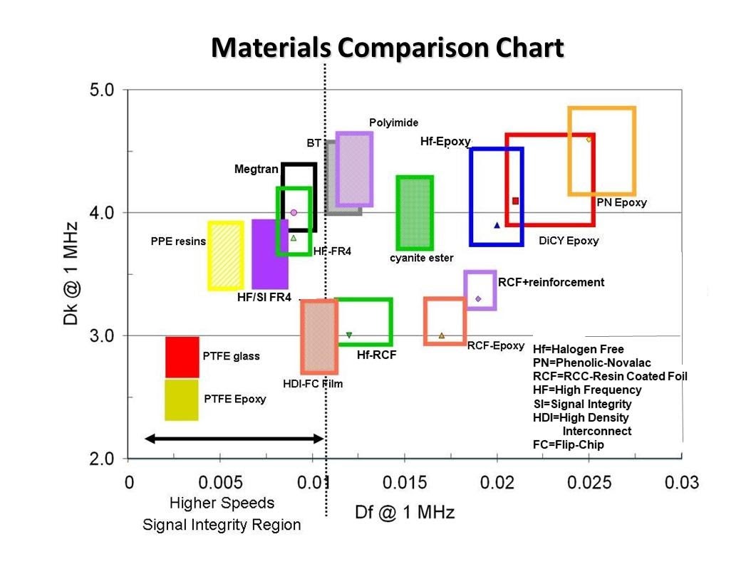
Impedance controlled routing maintains a consistent characteristic impedance along the trace length, crucial for high-speed signals. Engineers specify single-ended impedances around 50 ohms or differential at 100 ohms, calculated from stackup parameters like dielectric height and trace width. Variations from manufacturing tolerances demand design margins, often ±10%.
Stackup planning positions signal layers adjacent to ground planes for microstrip or stripline configurations. Wider traces for lower impedance or thinner dielectrics adjust values precisely. Field solvers verify calculations before layout.
Pitfalls include etch variations altering effective width, addressed by test coupons on panels. Consistent routing widths and spaces uphold control throughout.
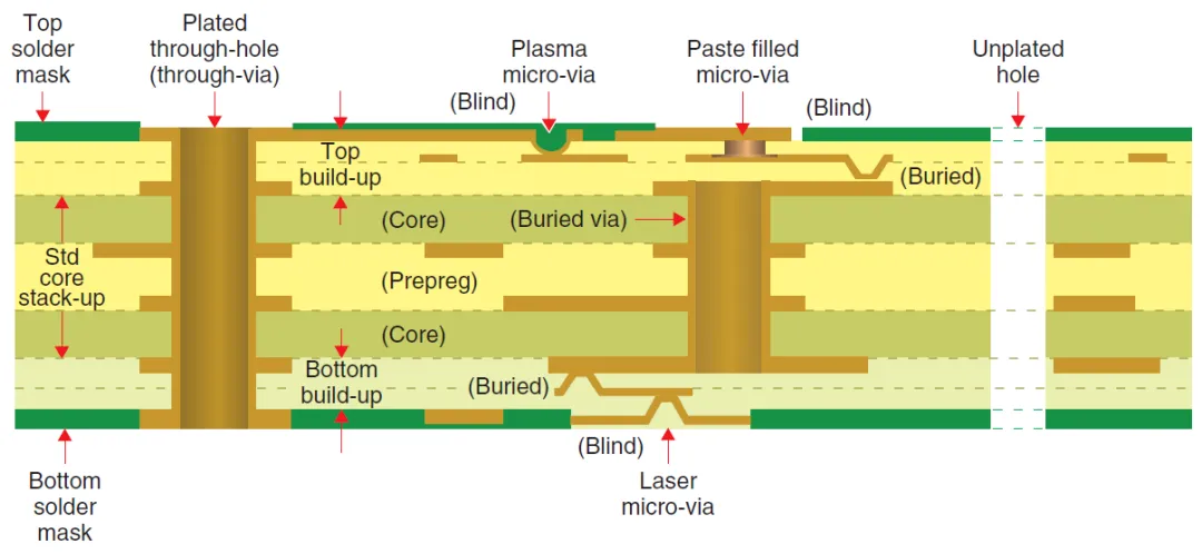
Strategies for Avoiding Vias in High-Speed Traces
Vias introduce impedance discontinuities due to their inductance and capacitance, causing reflections in high-speed traces. Each via adds about 1 nH of inductance, degrading signals above 1 GHz. Electric engineers minimize vias by planning component placement to keep critical nets on single layers.
When vias are necessary, use blind or buried types to reduce stubs. Backdrilling removes unused via portions, minimizing reflections. Pair vias with nearby ground vias for return current paths.
Routing high-speed traces avoids crossing plane splits, as detoured return currents increase loop inductance. Pre-layout analysis identifies via-heavy paths for redesign. These strategies preserve signal fidelity.
Techniques for Minimizing Trace Length
Minimizing trace length reduces propagation delay and attenuation, essential for timing-critical signals. Shorter paths limit exposure to crosstalk and EMI pickup. Engineers position drivers and receivers close together during placement.
Direct routing avoids detours, using fanouts optimized for minimal length. For unmatched requirements, serpentine meanders equalize pairs without excessive coupling. Constraints enforce maximum lengths during autorouting.
In dense boards, hierarchical routing prioritizes critical nets first. Post-route verification measures actual lengths against specs. This approach ensures synchronized arrivals.
Optimizing Ground Plane Routing
Ground plane routing provides a low-impedance return path directly beneath signal traces, reducing loop area and EMI. Solid planes on inner layers shield signals and stabilize references. Engineers avoid splits under high-speed areas; if unavoidable, use stitching vias every quarter wavelength.
Power planes complement grounds but require decoupling to prevent noise coupling. Clearance cutouts around vias maintain plane integrity. Multiple ground planes in thick stackups distribute currents evenly.
Flood fills connect fragmented grounds, ensuring continuity. These practices enhance overall integrity.
Common Pitfalls and Troubleshooting Insights
A frequent pitfall is routing high-speed traces over plane splits, forcing return currents to detour and increase inductance. Engineers detect this via simulation, observing eye diagram closure. Another issue: 90-degree bends create resonances; opt for chamfered corners instead.
Crosstalk from under-spaced parallels shows as glitches on scopes. Increase separation or add shields. Via stubs cause ringing; backdrill or eliminate them.
Impedance drifts from fab variations require coupons for verification. Per IPC-6012 performance specs, controlled processes yield consistent results. Systematic checks post-layout catch these early.
In a typical high-speed design, iterative simulation-refine cycles resolve most issues before fab.
Conclusion
Effective PCB routing hinges on integrating differential pair routing, impedance controlled routing, avoiding vias in high-speed traces, minimizing trace length, and ground plane routing. These techniques, grounded in transmission line principles, mitigate reflections, crosstalk, and EMI for reliable high-speed performance. Electric engineers benefit from early planning, simulation, and standard adherence like IPC-2221 guidelines. Implementing them systematically reduces risks and iterations. Prioritize these in your next design to achieve superior signal integrity.
FAQs
Q1: What is differential pair routing and why is it essential for signal integrity?
A1: Differential pair routing involves two traces carrying complementary signals with tight coupling and length matching. It rejects common-mode noise, vital for high-speed interfaces. Maintain constant spacing and symmetric routing to avoid skew. This technique aligns with impedance controlled routing for optimal performance. Engineers use it to ensure data integrity in GHz applications.
Q2: How do you implement impedance controlled routing in multilayer PCBs?
A2: Start with stackup definition to calculate trace widths for target impedance, like 50 ohms single-ended. Route signals adjacent to ground planes for stable reference. Verify with field solvers and include test structures. Avoid discontinuities to preserve control. This prevents reflections, enhancing overall signal integrity.
Q3: Why is avoiding vias in high-speed traces important, and what alternatives exist?
A3: Vias disrupt impedance and add inductance, causing signal reflections at high frequencies. Minimize them through strategic placement reducing layer changes. Use blind or buried vias or backdrilling as alternatives. Ground stitching supports return paths. These steps maintain waveform quality in critical nets.
Q4: How does ground plane routing improve minimizing trace length effects?
A4: Ground planes provide short return paths, reducing loop inductance alongside shorter traces. Stitch planes to handle current spreading. Avoid splits under signals for continuous reference. This combination minimizes delay skew and EMI. Integrate with length matching for timing precision.
References
IPC-2221A — Generic Standard on Printed Board Design. IPC
IPC-2141 — Controlled Impedance Design Guidelines. IPC
IPC-6012E — Qualification and Performance Specification for Rigid Printed Boards. IPC, 2017