What is PDN Impedance and Why is it So Important?
PDN impedance, or Power Distribution Network impedance, refers to the resistance encountered by alternating current (AC) within a printed circuit board's (PCB) power delivery system. The PDN's fundamental role is to supply stable and clean power to all active components on the board. Its impedance directly influences the network's ability to manage sudden current demands (transients) and maintain a consistent voltage level. Elevated impedance can lead to voltage fluctuations (noise), and potentially trigger signal integrity issues, whereas a low impedance PDN ensures superior power delivery and enhanced overall performance.
Effective power integrity design critically depends on controlling PDN impedance to prevent problems such as electromagnetic interference (EMI) and noise on the power rails. With contemporary electronic devices operating at increasingly higher speeds and lower voltages (often below 1V for advanced integrated circuits), even minor voltage fluctuations, like a 50mV ripple, can cause significant operational issues. This makes the mastery of PDN impedance a paramount concern for engineers engaged in high-speed or high-performance electronics design.
Defining a PDN Impedance Target for Optimal Performance
A crucial initial step in power integrity design involves establishing a specific PDN impedance target. This target represents the maximum permissible impedance that guarantees voltage noise remains within acceptable limits, even during peak transient current demands. For example, if a processor suddenly draws a 10A current spike, the PDN must ensure the voltage remains stable within a predefined tolerance (e.g., ±5%, which equates to 50mV for a 1V power rail). The target impedance can be calculated using a straightforward formula:
Z_target = ΔV / I_transient
Here, ΔV signifies the maximum allowable voltage ripple, and I_transient denotes the maximum transient current. For a 1V power rail with an allowed 50mV ripple and a 10A transient current, the target impedance would be 5mΩ (0.05V / 10A). Achieving such a low impedance across a broad frequency spectrum (from DC to several GHz) presents a considerable design challenge, yet it is absolutely critical for modern, high-performance designs.
Establishing a realistic PDN impedance target is contingent upon the specific requirements of your components, including the power supply characteristics and the sensitivity of various ICs to noise. Begin by reviewing component datasheets for specified noise margins and current profiles, then use these figures to define your precise target.
Techniques for PDN Impedance Measurement
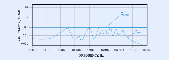
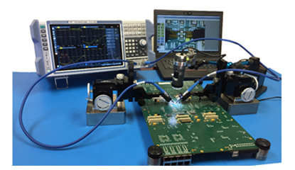
Once an impedance target has been defined, the subsequent crucial step is to perform PDN impedance measurement to confirm that your design meets the specified requirements. This measurement process typically employs specialized equipment such as a Vector Network Analyzer (VNA) or an oscilloscope paired with a low-noise probe. These instruments are invaluable for analyzing the impedance profile across a range of frequencies, helping to identify potential issues like resonance peaks that could amplify unwanted noise.
To accurately measure PDN impedance, follow these procedural steps:
● Setup Preparation: Connect the VNA or measurement device to designated test points on the power rail. It is vital to ensure that the setup minimizes interference from external noise sources.
● Frequency Sweep: Conduct a frequency sweep from very low frequencies (a few Hz) up to high frequencies (1GHz or beyond) to capture the complete impedance profile of the PDN.
● Result Analysis: Carefully examine the measurement results for any regions where the impedance exceeds your target. Pay particular attention to frequencies that correspond to the switching speeds of your ICs (e.g., 100MHz for a high-speed processor).
Accurate measurement often necessitates a carefully controlled environment to mitigate parasitic effects introduced by probes or test fixtures. For instance, if a resonance peak appears at 50MHz with an impedance of 100mΩ—significantly above your 5mΩ target—it strongly indicates the need for design modifications, such as the strategic addition of decoupling capacitors.
Related Reading: DIY PCB Impedance Measurement: A Home Lab Guide
Strategies for Designing a Low Impedance PDN
A low impedance PDN forms the bedrock of robust power integrity. The objective is to maintain the impedance below the defined target across the entire operating frequency spectrum, thereby minimizing voltage fluctuations and noise. Here are several proven strategies to achieve a low impedance PDN:
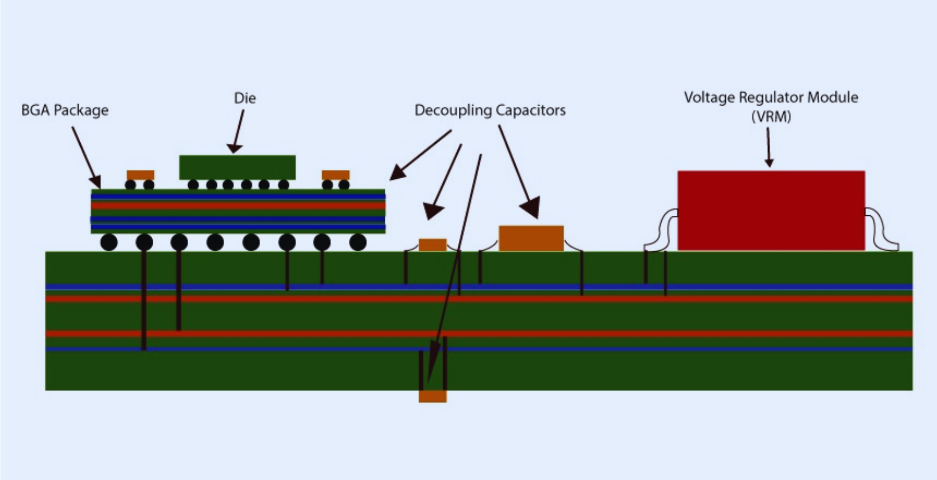
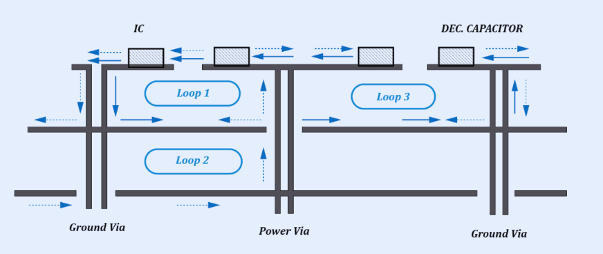
● Strategic Decoupling Capacitors: Incorporate decoupling capacitors of various values (e.g., 0.1μF, 1μF, and 10μF) placed in close proximity to the power pins of ICs. These capacitors act as local energy reservoirs, effectively reducing impedance at higher frequencies.
● Optimized Power Plane Design: Design power and ground planes as closely spaced layers (e.g., 5-10 mils apart) to create a low-inductance path. This configuration can reduce the overall PDN impedance by as much as 50% compared to designs with wider plane spacing.
● Minimizing Via Inductance: Utilize multiple vias for power connections to significantly lower parasitic inductance. While a single via might contribute 1nH of inductance, employing four vias in parallel can reduce this to approximately 0.25nH.
● Shortening Trace Lengths: Keep all power traces as short as physically possible. This directly reduces parasitic inductance and resistance, which are key contributors to overall impedance.
By combining these techniques, designers can achieve a low impedance PDN that ensures stable power delivery, even under challenging conditions such as a 20A current surge.
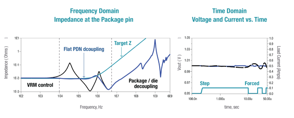
Utilizing PDN Impedance Simulation for Design Validation
Before proceeding to PCB manufacturing, executing a PDN impedance simulation is an indispensable step to predict performance and identify potential issues early in the design cycle. Simulation tools allow designers to model the entire PDN and analyze its impedance profile virtually, thereby saving considerable time and cost associated with building physical prototypes.
Here’s a structured approach to PDN impedance simulation:
● Model Construction: Create a detailed schematic or layout model of your PDN. This should include all power planes, vias, decoupling capacitors, and the power pins of integrated circuits. Crucially, incorporate parasitic elements such as trace inductance (e.g., 0.5nH per inch) and capacitor Equivalent Series Inductance (ESL), which is often around 1nH.
● Frequency Range Definition: Set the simulation's frequency range from DC up to several gigahertz to encompass all relevant operating frequencies for your design.
● Impedance Curve Analysis: Carefully examine the simulated impedance curve. Look for any peaks that exceed your target impedance. For example, a peak at 200MHz with an impedance of 20mΩ against a 5mΩ target clearly signals a resonance issue.
● Iterative Design Adjustments: Based on simulation results, iteratively adjust capacitor values, plane spacing, or via configurations within the simulation environment to flatten the impedance curve and bring it within acceptable limits.
Simulation is a powerful validation tool that empowers early design refinement. Many engineers find that optimizing capacitor placement and values in simulation can reduce high-frequency impedance by 30-40%, effectively averting costly redesigns post-manufacturing.
Related Reading: 6-Layer PCB Power Distribution Networks: Design for Low Noise and High Efficiency
PDN Impedance Optimization: Fine-Tuning for Peak Performance
PDN impedance optimization extends beyond initial design—it involves the meticulous fine-tuning of the power delivery network to effectively suppress noise and achieve stringent performance objectives. As chip sizes continue to shrink and transistor counts soar (often exceeding 10 billion in advanced ICs), power integrity challenges intensify, making optimization absolutely critical.
Consider incorporating these optimization techniques:
● Multi-Layer Decoupling Strategy: Employ a layered approach to decoupling, utilizing a combination of bulk capacitors (e.g., 100μF for very low frequencies), mid-range capacitors (e.g., 10μF for mid-frequencies), and small, high-frequency capacitors (e.g., 0.1μF for high frequencies). This comprehensive strategy helps to cover the entire frequency spectrum, potentially reducing impedance peaks by up to 60% at critical frequencies.
● Anti-Resonance Management: Actively identify and suppress anti-resonance spikes, which are typically caused by unwanted interactions between capacitors and inductances. This can be achieved by adjusting capacitor values or by adding damping resistors (e.g., 0.5Ω in series with a capacitor).
● Targeted Impedance Tuning: Focus your optimization efforts on the specific frequencies where your integrated circuits are most active. For a 500MHz processor, prioritize achieving a very low impedance around 500MHz and its harmonics (1GHz, 1.5GHz).
Optimization is an iterative process that often integrates both simulation and physical measurement. For example, after simulation reveals a 30mΩ peak at 100MHz, you might strategically add a 1μF capacitor near the affected IC, then proceed to measure the real board to confirm that the impedance has dropped to the desired 5mΩ target. This meticulous, iterative process ensures that the PDN fully meets all power integrity requirements.
Common Challenges in PDN Impedance Design and Solutions
Designing for optimal PDN impedance presents its own set of challenges. Here are some frequently encountered issues and practical solutions:
● Resonance Peaks: These occur when complex interactions between capacitors and inductances amplify impedance at specific frequencies.
○ Solution: Address this by carefully adjusting capacitor placement and values, or by strategically adding damping elements like resistors.
● High-Frequency Noise: At frequencies exceeding 1GHz, parasitic effects become dominant and can significantly impact performance.
○ Solution: Utilize smaller capacitors (e.g., 0.01μF) characterized by very low Equivalent Series Inductance (ESL) and place them as close as physically possible to the power pins of sensitive ICs.
● Space Constraints: Modern, compact designs frequently present limitations on the available space for multiple decoupling capacitors.
○ Solution: Prioritize the placement of capacitors in high-impact locations near critical ICs. Additionally, explore the use of embedded capacitance within multi-layer board constructions to conserve valuable surface area.
Effectively addressing these challenges requires a judicious balance of theoretical knowledge, advanced simulation techniques, and thorough real-world testing to ensure the development of a robust and reliable PDN.
Conclusion: Achieving Superior PCBs Through PDN Impedance Mastery
Mastering PDN impedance is an essential cornerstone of effective power integrity design. By diligently setting a clear PDN impedance target, conducting precise PDN impedance measurement, thoughtfully designing a low impedance PDN, effectively leveraging PDN impedance simulation, and committing to ongoing PDN impedance optimization, engineers can guarantee stable power delivery and minimize unwanted noise in their PCB designs. These steps are particularly vital as electronic devices continue to increase in speed and complexity, demanding ever-tighter control over voltage stability.
At AIVON, we are dedicated to providing engineers with the resources and specialized services necessary to successfully navigate power integrity challenges. Whether your project involves a high-speed processor board or a compact IoT device, a deep understanding and precise control over PDN impedance will undeniably elevate your designs to an unparalleled level of performance. Begin implementing these advanced strategies in your next project to achieve consistently reliable and high-performance results.


