Introduction
Flex and rigid-flex printed circuit boards represent a significant advancement in PCB technology, allowing engineers to create compact, reliable interconnects for applications where space constraints and mechanical flexibility are critical. These designs combine the structural integrity of rigid boards with the bendability of flexible substrates, making them ideal for devices in medical wearables, aerospace systems, and automotive electronics. However, designing flex and rigid-flex PCBs introduces unique challenges, such as managing material transitions, controlling mechanical stress during bending, and ensuring signal integrity across varying sections. Common pain points include defining precise board outlines, optimizing layer stack-ups, selecting appropriate adhesives, and preparing for reliable bending assembly. Addressing these issues requires a deep understanding of material properties and fabrication processes to avoid failures like delamination or trace cracking. By following structured engineering approaches, designers can overcome these hurdles and deliver high-performance boards that meet demanding reliability requirements.
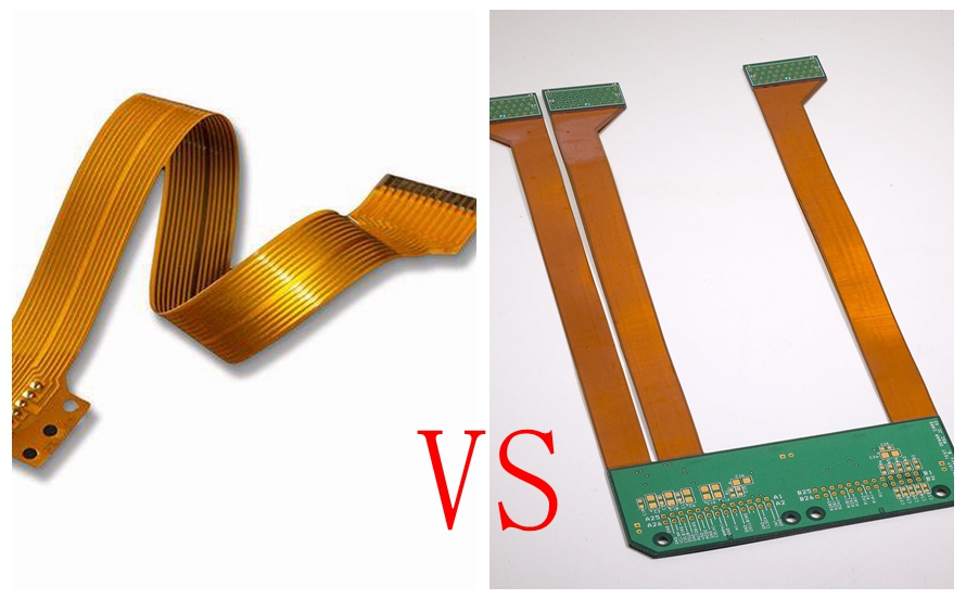
What Is Flex-Rigid Design and Why It Matters
Flex-rigid design, often referred to as rigid-flex PCB construction, integrates rigid multilayer sections with flexible single- or double-sided tails or bridges, enabling three-dimensional assembly in tight spaces. Flexible sections typically use polyimide films as the base material, which provide excellent thermal stability and bend endurance compared to rigid FR4 substrates. Rigid areas maintain standard multilayer stack-ups for component mounting and high-density routing, while flex regions facilitate movement or folding during final assembly. This hybrid approach matters in modern electronics because it reduces connector counts, minimizes weight, and enhances vibration resistance in dynamic environments. For electric engineers, mastering flex-rigid design ensures compliance with performance specs and extends product lifespan in harsh conditions. Ultimately, these boards bridge the gap between form factor limitations and functional demands.
Suggested Reading: Flexible and Rigid-Flex PCBs: The Complete Engineering Guide
Key Technical Challenges in Flex-Rigid Design
One primary challenge in flex-rigid design lies in defining the board outline, particularly at the transitions between rigid and flexible zones. Engineers must account for manufacturing tolerances, as flex areas require precise cutouts to prevent tearing or misalignment during lamination. Irregular outlines in flex tails can lead to uneven stress distribution, exacerbating risks during repeated bending. Layer stack-ups present another complexity, with rigid sections featuring cores and prepregs juxtaposed against flex laminates that use coverlays and adhesives. Mismatched coefficients of thermal expansion between materials can cause warpage or delamination post-fabrication. Signal propagation also varies, demanding careful impedance control across the stack-up to maintain high-speed performance.
Adhesive selection and types of layer-ups for adhesive further complicate the process. Traditional adhesive-based constructions bond copper foils to polyimide using acrylic or epoxy adhesives, but these can introduce thickness variability and reduce flexibility over time. Adhesiveless builds, where copper is directly laminated to polyimide via sputtering, offer superior bend endurance but increase costs and limit layer counts. In multilayer flex-rigid designs, engineers must balance these options while ensuring interlayer registration. Bending assembly introduces mechanical strain, where insufficient bend radii lead to copper cracking or substrate fatigue. IPC-2223 provides guidelines for bend radii and trace routing in flex zones to mitigate these risks.

Environmental factors amplify these challenges during assembly and operation. Moisture absorption in adhesives can cause blistering under reflow, while thermal cycling stresses transitions. Fabricators often recommend controlled baking to precondition materials, but design must anticipate these processes. Trace density in flex areas must avoid sharp bends, as copper ductility decreases with thinning. Vias at rigid-flex interfaces require staggered placement to prevent cracking under flexure. Overall, these interconnected issues demand iterative simulation and prototyping to validate designs.
Practical Solutions and Best Practices
To overcome board outline challenges, start by defining flex regions with smooth, curved transitions rather than sharp corners, incorporating strain-relief fillets at bends. Use mechanical cutouts or scored lines for precise separation post-lamination, allowing for 0.1 mm tolerances in high-volume production. Simulate outline stresses using finite element analysis to predict failure points early. For layer stack-ups, develop region-specific configurations: rigid sections with standard buildup, flex tails with symmetric 1-2-1 or 2-2 constructions for balanced strain. Transition zones should employ bookbinder or butterfly stack-ups to align layers without air gaps. Always verify stack-up impedance through field solver tools, targeting controlled differentials in flex areas.
When considering types of layer-ups for adhesive, opt for adhesiveless in high-flex applications to minimize hysteresis and improve cycle life, reserving adhesive types for cost-sensitive static bends. Epoxy-based adhesives suit multilayer builds for better peel strength, while acrylics offer easier processing. IPC-6013 outlines qualification tests like peel adhesion and flex endurance to qualify these choices. Document stack-up details clearly, including coverlay overlaps of at least 0.25 mm beyond traces. Prototype with panel-level arrays to assess uniformity before full runs.

Bending assembly best practices focus on dynamic vs. static requirements. Implement minimum bend radii scaled to total flex thickness, with teardrop entries for traces entering bend zones. Route signals perpendicular to bend lines in outer layers, shifting critical nets inward. During assembly, use fixtures to control fold angles, avoiding over-bending beyond design limits. Post-assembly, conduct cyclic bend tests to confirm durability. Integrate stiffeners in rigid-flex junctions for added support without compromising flexibility.
Troubleshooting Common Issues in Flex-Rigid Designs
Designers often encounter warpage in prototypes due to asymmetric stack-ups or mismatched CTEs. Mitigate by symmetrizing flex sections and using low-CTE adhesives. Delamination at transitions signals poor surface prep; ensure plasma cleaning before lamination. Impedance discontinuities arise from varying dielectrics - model full stack-ups iteratively. For bending failures, inspect trace etch quality and copper weight; thinner foils (18 μm) excel in tight radii. Field failures from vibration highlight the need for anchored vias and ground planes in flex tails.
A practical case involved a medical device rigid-flex board failing cyclic bend tests. Root cause was inadequate coverlay adhesion in a 4-layer flex tail. Switching to an adhesiveless 2-2 stack-up and adding strain fillets resolved it, passing 100,000 cycles per IPC-6013 criteria.
Conclusion
Overcoming flex-rigid design challenges demands meticulous attention to board outlines, layer stack-ups, adhesive selections, and bending assembly processes. By applying logical stack-up strategies, adhering to proven guidelines like those in IPC-2223, and validating through testing, engineers can produce reliable, high-density interconnects. These practices not only enhance mechanical durability but also ensure electrical performance in compact applications. Prioritizing simulation and prototyping minimizes iterations, accelerating time-to-market. Ultimately, mastering these elements positions designs for success in demanding environments.
FAQs
Q1: What is Flex-Rigid Design, and how does it differ from pure flex PCBs?
A1: Flex-rigid design combines rigid multilayer sections for components with flexible polyimide tails for interconnects, unlike pure flex boards that lack rigid support. This hybrid enables 3D folding while maintaining structural integrity. Engineers benefit from reduced connectors and better vibration resistance. Proper layer stack-ups ensure seamless transitions.
Q2: How do layer stack-ups impact Flex-Rigid Design performance?
A2: Layer stack-ups in flex-rigid designs must balance rigid cores with flex laminates to control impedance and warpage. Symmetric constructions prevent delamination, while region-specific builds optimize signal integrity. Adhesives and coverlays dictate flexibility. Simulate full profiles for accuracy.
Q3: What are the main types of layer-ups for adhesive in flex-rigid PCBs?
A3: Common types include adhesive-based with acrylic or epoxy bonding copper to polyimide for cost-effective static use, and adhesiveless via direct lamination for dynamic bending. Adhesive builds suit multilayers; adhesiveless excels in endurance. Select per bend requirements.
Q4: What best practices address bending assembly in Flex-Rigid Design?
A4: Use scaled bend radii, perpendicular trace routing, and strain-relief fillets to minimize copper fatigue. Fixtures control assembly folds, while inner-layer signals avoid outer strain. Test cyclically for validation. This ensures long-term reliability.
References
IPC-2223C - Sectional Design Standard for Flexible Printed Boards. IPC, 2019
IPC-6013DS - Qualification and Performance Specification for Flexible and Rigid-Flex Printed Boards. IPC, 2020


