What Exactly Is Prepreg, and Why Is Its Thickness So Important in PCBs?
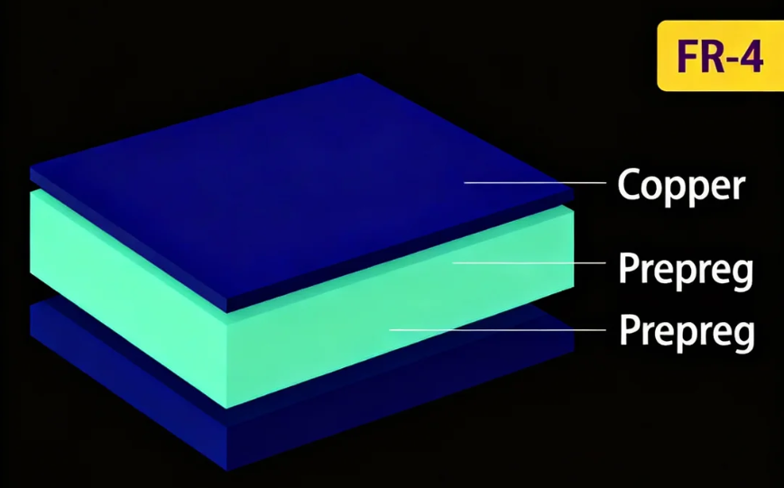
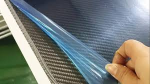
Prepreg, an abbreviation for "pre-impregnated," is a foundational material in the construction of multilayer Printed Circuit Boards (PCBs). It consists of a fiberglass fabric that has been saturated with a resin, typically epoxy, and then partially cured to a semi-solid, "B-stage" state. During the PCB lamination process, this material undergoes a critical transformation: under intense heat and pressure, the resin within the prepreg melts, flows, and then fully cures, acting as both an insulating layer and a powerful adhesive that bonds the individual copper layers together to form a robust, monolithic board structure.
The precise thickness of the prepreg layers is a critical design parameter, directly influencing several key performance characteristics of the finished PCB. It dictates the dielectric properties, which are essential for maintaining signal integrity, particularly for high-speed traces where impedance control is paramount. For example, a thinner prepreg layer between a signal trace and its reference plane can reduce the dielectric spacing, thereby affecting the characteristic impedance, which is often targeted at 50 ohms for many designs. Furthermore, appropriate prepreg thickness contributes significantly to the mechanical strength and structural integrity of the PCB, enabling it to endure physical stresses during assembly and throughout its operational life. It also plays a role in thermal management, impacting how effectively heat dissipates, especially in high-power applications. Finally, prepreg layers are major contributors to the overall thickness of the PCB, which must adhere to specific design specifications, such as the common 1.6mm for standard boards. Therefore, a thorough understanding and careful selection of prepreg thickness are fundamental to successful PCB stackup design, ensuring that both electrical and mechanical requirements are met.
How Does Prepreg Thickness Fit into Multilayer PCB Stackup Design?
PCB stackup design refers to the deliberate arrangement of the various copper layers and the insulating materials—cores and prepregs—within a multilayer circuit board. In this context, prepreg thickness is pivotal, as it directly controls the spacing between conductive layers, which in turn profoundly impacts signal performance and the overall manufacturability of the board.
Consider a typical 4 layer PCB board stackup: it usually consists of a top copper layer (for signals), followed by a prepreg layer, then an inner copper layer (often a ground plane), then a thicker core material, another inner copper layer (typically a power plane), another prepreg layer, and finally, a bottom copper layer (for signals). Prepreg layer thicknesses commonly fall within a range of 0.002 inches (2 mils) to 0.010 inches (10 mils), varying based on specific design needs. For designs involving high-speed signals, it's common practice to employ thinner prepreg layers, often around 3-5 mils, between signal and ground planes. This approach helps maintain tight impedance control, usually targeting a dielectric constant (Dk) of approximately 4.0 for standard FR-4 materials. The process of selecting the correct prepreg thickness for your stackup is a balancing act, weighing the demands of electrical performance against the realities of manufacturing feasibility. While thinner layers generally enhance signal integrity, they can also lead to increased manufacturing costs and complexity. Conversely, thicker layers are easier to process but might not meet the stringent tolerances required for advanced, high-frequency applications.

What Factors Influence the Choice of Prepreg Material and Thickness?
Selecting the most suitable prepreg material and its corresponding thickness is a pivotal decision that directly influences the functionality and reliability of a PCB design. Several critical factors must be carefully evaluated:
Electrical Performance Requirements
For high-speed or high-frequency designs, the paramount concern is minimizing signal loss. This necessitates the use of prepreg materials characterized by low dielectric constants (Dk) and low dissipation factors (Df). While standard FR-4 prepreg typically has a Dk ranging from 4.0 to 4.5, more advanced materials, such as polyimide or PTFE-based prepregs, can offer significantly lower Dk values (as low as 2.2), which are crucial for superior performance at frequencies exceeding 1 GHz. In these applications, thinner prepreg layers are often preferred to achieve precise impedance control, such as the common 50 ohms for single-ended traces.
Mechanical and Thermal Considerations
The total thickness of the finished PCB must comply with the mechanical constraints of the final product enclosure. If a design mandates a total board thickness of 1.6mm, for instance, a meticulous calculation is required to ensure that the cumulative thickness of all prepreg layers, alongside core and copper layers, aligns with this specification. Standard designs frequently utilize prepreg layers around 6-8 mils thick. For applications experiencing high power dissipation, thicker prepreg layers might offer enhanced thermal insulation between internal layers, helping to prevent heat buildup. Conversely, for designs prioritizing efficient heat transfer, thinner prepreg layers might be combined with strategically placed thermal vias.
Cost-Effectiveness and Availability
It's important to recognize that thinner prepreg materials and specialized resin systems, such as high-Tg (glass transition temperature) or low-Dk options, typically come with a higher price tag. Therefore, designers must carefully balance the required performance characteristics with budget limitations, particularly for products intended for mass production. It is always advisable to consult with your chosen PCB manufacturing partner to confirm that the selected materials and thicknesses are compatible with their fabrication processes and readily available.
Understanding Prepreg Thickness Tolerances in Manufacturing
Prepreg thickness tolerances refer to the acceptable range of variation in the material's thickness during the manufacturing process. These tolerances are critically important because even slight deviations can have a ripple effect, impacting impedance characteristics, signal integrity, and the physical fit of the PCB within its designated enclosure.
For standard FR-4 prepreg, the large PCB manufacturer typically specifies a tolerance of ±10% of the nominal thickness. This means a nominal 6-mil prepreg layer could vary anywhere between 5.4 mils and 6.6 mils. However, during the complex lamination process—influenced by factors like applied pressure, temperature, and resin flow—further variations can occur. This might result in an overall final board thickness tolerance, for example, of ±0.15mm for a 1.6mm thick board. For designs demanding high precision, such as those used in RF or cutting-edge high-speed digital applications, tighter tolerances are often necessary. In these scenarios, designers might need to specify prepreg with a stricter tolerance of ±5% or opt for advanced materials engineered for more consistent thickness control. It's crucial to acknowledge that demanding tighter tolerances can lead to increased manufacturing costs, so this should be factored into the project budget. To manage tolerances effectively, it's essential to include detailed stackup specifications in your design files, clearly outlining acceptable thickness ranges for each layer. Furthermore, utilizing impedance simulation tools can help predict how variations in prepreg thickness might affect signal performance; for example, a 10% deviation in a 4-mil prepreg layer could shift impedance by 2-3 ohms, potentially leading to signal mismatches. Lastly, maintaining proactive communication with your manufacturing partner is vital to confirm their capabilities in meeting your specified tolerance requirements.
Exploring Different Types of Prepreg for PCB Designers
Prepreg materials come in a diverse range of types, each engineered to suit specific application requirements. Familiarizing yourself with these options is crucial for making informed design decisions.
General-Purpose and High-Performance Prepregs
Standard FR-4 Prepreg is the most widely adopted material, offering a balanced combination of cost-effectiveness and performance. It typically features a glass transition temperature (Tg) around 130-140°C and a dielectric constant (Dk) of 4.0-4.5, making it suitable for a broad spectrum of general-purpose applications, including consumer electronics. Common thicknesses span from 3 to 10 mils.
High-Tg Prepreg boasts a Tg of 170-180°C or higher, providing superior thermal stability. This makes it ideal for applications exposed to elevated operating temperatures, such as automotive or industrial control systems, where enhanced reliability in harsh environments justifies its slightly higher cost.
Low-Dk/Low-Df Prepreg is specifically formulated for high-frequency and high-speed digital designs. These materials are engineered to minimize signal loss and distortion, often featuring Dk values below 3.5. They are indispensable in critical applications like RF, microwave, and 5G communication systems, where thicknesses are usually kept very thin (2-5 mils) to achieve precise impedance control.
Specialized and Eco-Friendly Prepregs
Halogen-Free Prepreg is an environmentally conscious choice, as it avoids the use of harmful halogenated chemicals. It is increasingly specified in consumer products to comply with directives such as RoHS, although its mechanical properties might differ subtly from standard FR-4.
Flexible Prepreg is integral to the fabrication of flexible and rigid-flex PCBs. These materials are designed to withstand repeated bending without compromising structural or electrical integrity, typically made from polyimide resins. They are widely used in compact electronics, wearable devices, and medical implants where conformability is essential. Each prepreg type serves a distinct purpose, necessitating a selection based on the specific electrical, thermal, and mechanical demands of your project. For highly advanced designs, it is also possible to create "hybrid stackups" by combining different prepreg types within a single board to leverage their varied properties across different layers.
Suggested Reading: PCB Prepreg Thickness: A Designer's Guide to Stackup, Materials, and Performance
Best Practices for Integrating Prepreg Thickness into Your Design Workflow
To ensure optimal performance and manufacturability in your PCB designs, integrating these best practices related to prepreg thickness is crucial:
● Early Simulation is Key: Utilize PCB design software with stackup analysis capabilities to simulate various configurations. This allows you to accurately predict impedance based on chosen prepreg thicknesses. For example, simulating a 5-mil prepreg layer between a signal trace and a ground plane on FR-4 material can help determine the precise trace width (e.g., 6 mils) needed to achieve a 50-ohm impedance.
● Account for Resin Flow: During the lamination process, the prepreg resin will flow under heat and pressure, which can subtly alter the final dielectric thickness. Establish clear communication with your manufacturing partner to understand their specific process and adjust your design as necessary to compensate for this effect.
● Prioritize Standard Materials: Whenever possible, choose commonly available prepreg thicknesses (such as 4, 6, or 8 mils). This approach can significantly reduce both manufacturing costs and lead times, reserving custom specifications only for designs with absolute critical requirements.
● Consider Layer Count Implications: An increased number of layers in your PCB stackup directly translates to more prepreg material, which adds to the overall board thickness. Carefully plan your stackup to prevent exceeding mechanical dimension constraints of the final product.
● Prototype and Validate: Always build and thoroughly test prototypes, especially for critical applications. This iterative step allows you to verify that your chosen prepreg thicknesses and materials indeed meet all specified performance expectations.
Common Hurdles with Prepreg Thickness and Their Solutions
Even with meticulous planning, certain challenges related to prepreg thickness can surface during PCB design and manufacturing. Here are some prevalent issues and their practical solutions:
● Impedance Mismatch: Inconsistent prepreg thickness can lead to deviations from target impedance values, compromising signal integrity. The primary solution involves specifying tightly controlled dielectric materials and strict thickness tolerances during fabrication.
● Delamination Risk: If prepreg layers are excessively thin or their properties are incompatible with adjacent materials, the board can suffer delamination, particularly under thermal cycling. To counteract this, select materials with closely matched coefficients of thermal expansion (CTE) and ensure adequate resin content in the prepreg.
● Excessive Board Thickness: The cumulative thickness of multiple prepreg layers can sometimes push the total board thickness beyond design limits. This challenge can be addressed by optimizing the stackup, potentially utilizing thinner prepreg variants, or reconsidering the total number of layers if feasible.
Proactive and open communication with your chosen PCB manufacturing partner is an invaluable strategy. Engaging them early in the design phase allows for the identification and resolution of these challenges, ultimately saving significant time, effort, and resources in the long run.
Conclusion: Mastering Prepreg Thickness for Superior PCB Designs
Prepreg thickness is a foundational and indispensable aspect of Printed Circuit Board design, exerting a profound influence on everything from critical signal integrity to overall mechanical durability. By cultivating a deep understanding of how to judiciously select the appropriate prepreg material, construct efficient and effective stackups, skillfully manage manufacturing tolerances, and choose the correct prepreg type for each application, designers can consistently create highly reliable and robust PCBs precisely tailored to their specific needs.
Whether your current project involves a straightforward 2-layer board or a sophisticated, high-speed multilayer design, giving meticulous attention to prepreg thickness will unequivocally elevate the caliber of your work. Leverage the insights, strategic approaches, and best practices shared within this guide as a robust starting point to refine your design methodology and achieve consistently exceptional results in every project you undertake.


