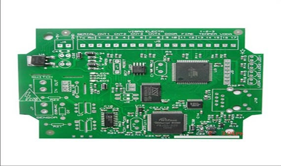
Why is Thoughtful Router PCB Design So Important?
Router Printed Circuit Boards (PCBs) form the foundational hardware for all networking devices, orchestrating data traffic flow between various networks. A meticulously designed PCB is crucial for ensuring stable performance, minimizing unwanted signal interference, and facilitating efficient power management. For those new to electronics design, comprehending the specific challenges inherent in router PCB development—such as the precise routing of high-speed signals, accurate impedance matching, and effective thermal dissipation—is paramount. A poorly executed design can lead to frustrating consequences, including frequent dropped network connections, sluggish data transfer rates, or even complete hardware failure.
This guide is specifically tailored to assist hobbyists, students, and early-career engineers in grasping the fundamental principles of designing PCBs specifically for router applications. By adhering to the outlined steps, you will acquire the necessary skills to construct a board that reliably meets basic networking requirements while adeptly avoiding common design pitfalls.
Initial Steps: Grasping the Core Concepts of Router PCB Design
Before delving into the intricate design process, it is essential to establish a foundational understanding of router PCB characteristics. A typical router PCB integrates key components such as a microprocessor or microcontroller (for data processing), Ethernet controllers (for network connectivity), sophisticated power management circuitry, and various connectors for external interfaces. The board's layout must be engineered to proficiently handle high-speed signals, which often range from 100 MHz to several gigahertz, depending on the router's performance capabilities.
For beginners, it's advisable to commence with a straightforward design objective, such as a single-band Wi-Fi router intended for basic internet routing. This approach effectively reduces complexity, allowing you to focus on mastering critical concepts like signal integrity and efficient power distribution. As a general guideline, aim for a design that can support data rates of at least 100 Mbps for a fundamental router; this target is readily achievable using cost-effective components and standard PCB manufacturing processes.
What Differentiates Router PCB Design?
Unlike generic PCBs, router designs place a heightened emphasis on optimizing high-speed signal pathways and ensuring excellent electromagnetic compatibility (EMC). Signals must propagate cleanly without interference, and traces require meticulous routing to prevent crosstalk. Moreover, routers frequently necessitate multi-layer boards (typically four or more layers) to physically separate power planes, ground planes, and various signal layers, thereby guaranteeing pristine operational performance.
Defining the Functional Requirements of Your Router
Every successful PCB design project begins with a meticulously defined set of requirements. It is crucial to articulate precisely what functions your router needs to perform. Will it solely support wired connections, or will it incorporate wireless (Wi-Fi) capabilities? What specific data transfer speeds are you targeting? For an initial beginner project, consider these fundamental specifications:
Example Router Specifications for Beginners
● Data Speed: A starting point of 100 Mbps (Fast Ethernet) is highly recommended.
● Ports: Include 1 WAN (Wide Area Network) port and 2-4 LAN (Local Area Network) ports.
● Power Input: Design for a standard 5V or 12V input with a current rating of 1-2A.
● Wi-Fi Capability (Optional): If wireless functionality is desired, begin with a single-band 2.4 GHz implementation.
Documenting these specifications meticulously will serve as a clear roadmap, guiding both your component selection and schematic design phases. This proactive step helps to prevent "scope creep" and ensures your project remains manageable and achievable.
Related Reading: Designing Your First Router PCB: A Beginner's Comprehensive Guide
Thoughtful Component Selection for Router PCBs
The selection of appropriate components is a pivotal phase in router PCB design. For novice designers, it’s best to prioritize widely available parts that come with comprehensive documentation and benefit from robust community support. Here’s a breakdown of essential component categories:
Key Component Categories
● 1. Microcontroller or System on Chip (SoC): This component acts as the central processing unit of your router, responsible for data processing and routing. For a basic design, choose a chip that offers integrated Ethernet support and possesses adequate processing power (ee.g., a clock speed of 100-300 MHz). Look for development boards or existing reference designs as these can significantly simplify the integration process.
● 2. Ethernet Controllers and Physical Layer Devices (PHYs): These components manage the wired network connections. For simplicity, select parts that support 10/100 Mbps Ethernet. Crucially, ensure that the PHY (Physical Layer Device) is compatible with your chosen microcontroller’s interface, which is often SPI or MII.
● 3. Power Management Integrated Circuits (PMICs): Routers demand stable power delivery, frequently necessitating voltage regulators to step down the input voltage (e.g., converting 12V to 3.3V or 1.8V for digital circuitry). Opt for regulators that can supply at least 1.5A output current to comfortably handle peak operational loads.
● 4. Connectors and Passive Components: Utilize standard RJ45 connectors for your Ethernet ports. Ensure that all capacitors and resistors selected match the specific voltage and current ratings defined in your design. For managing high-speed signals, it’s advisable to use decoupling capacitors with a low Equivalent Series Resistance (ESR), typically 0.1 μF, placed in close proximity to the IC power pins.
Designer's Tip: Always consult the comprehensive datasheets for each component to verify pin compatibility, precise power requirements, and recommended operating conditions. Mismatched components are a frequent cause of design failures.
Crafting the Schematic Diagram for Router PCBs
Once all components have been meticulously selected, the next crucial step is to create a schematic diagram. This diagram serves as the electrical blueprint, illustrating how all components are interconnected. This phase is absolutely vital for confirming electrical correctness before advancing to the physical PCB layout.
Effective Schematic Design Practices
● Functional Organization: Group related components into logical blocks (e.g., power supply, processor core, Ethernet interface) to enhance clarity and ease of understanding.
● Leverage Reference Designs: Many semiconductor manufacturers provide sample schematics for their chips. Adapt these proven designs to fit your specific project requirements.
● Strategic Decoupling Capacitors: Place 0.1 μF decoupling capacitors in close proximity to the power pins of all integrated circuits (ICs) to effectively filter out high-frequency noise.
● Clear Net Labeling: Assign meaningful names to all electrical connections (e.g., “VCC_3.3V”, “ETH_TX+”) to prevent errors during the subsequent PCB layout phase.
For a router schematic, it is particularly important to clearly mark high-speed signal paths, such as Ethernet lines, to indicate they require differential pair routing later. A standard Ethernet connection typically demands precise impedance matching, often 100 ohms for differential pairs, which must be clearly specified within your schematic.
Selecting the Optimal PCB Design Software
Your choice of PCB design software is the primary tool for translating your schematic into a physical board layout. For beginners embarking on router PCB design, it's essential to select software that offers a good balance between user-friendliness and crucial features like multilayer support and robust design rule checks (DRC).
Key Software Features to Prioritize
● Schematic Editor: A dedicated interface for drawing and connecting your circuit components.
● Layout Editor: A powerful environment for physically placing components and routing electrical traces on the board.
● Design Rule Checks (DRC): An automated system to identify and flag common errors such as incorrect trace widths, insufficient spacing, or unconnected nets.
● Extensive Library Support: Access to a comprehensive collection of component footprints and schematic symbols.
● Flexible Export Options: The ability to generate industry-standard Gerber files, which are necessary for PCB manufacturing.
Several popular software options offer free versions tailored for hobbyists or students, providing ample features for designing a basic router. Dedicate time to thoroughly learn the software through available tutorials to minimize potential delays in your project timeline.
Fundamental PCB Layout Techniques for Routers
With your schematic design finalized, the next critical step is to execute the PCB layout. This involves the precise placement of components and the routing of electrical traces across the board. For router PCBs, the layout directly influences overall performance, largely due to the presence of high-speed signals and demanding power requirements.
Essential Layout Best Practices for Beginners
● Multilayer Board Utilization: A 4-layer PCB is commonly used for router designs, typically allocating layers for high-speed signals, a dedicated ground plane, a stable power plane, and additional signal routing. This configuration is highly effective for noise reduction and signal isolation.
● Logical Component Placement: Strategically place high-speed components, such as Ethernet PHYs, as close as possible to their respective connectors. This minimizes trace lengths, which is crucial for signal integrity.
● Differential Pair Routing: Ethernet signals frequently utilize differential pairs. It is paramount to maintain equal trace lengths and consistent spacing (typically 5-10 mils apart) within these pairs to achieve the required 100-ohm differential impedance.
Related Reading: Mastering Differential Pair Routing for High-Speed PCB Design
● Dedicated Ground Plane: Dedicate an entire inner layer of your PCB to a solid ground plane. Connect all ground pins of components directly to this plane using short vias, which significantly reduces noise and provides a stable reference.
● Appropriate Trace Widths: Employ wider traces for power distribution (e.g., 20-30 mils for currents up to 1A) to minimize voltage drop, and narrower traces for general signals (e.g., 6-10 mils) where current is low.
For a beginner-level router design, aim for a board size of approximately 100mm x 100mm. This keeps manufacturing costs manageable while accommodating all essential components. Always utilize the design rule check (DRC) feature in your software to ensure that trace widths, spacing, and other parameters comply with the minimum manufacturing standards (e.g., minimum 6-mil trace width for most fabricators).
Design Validation, Testing, and Manufacturing Your PCB
Before committing your design to fabrication, thorough validation is indispensable. Once manufactured, rigorous testing confirms functionality.
Validation and Testing Procedures
● Design Rule Check (DRC): Run a comprehensive DRC in your PCB software to identify and rectify any errors, such as unconnected pins or incorrect spacing between traces.
● Signal Integrity Simulation (Optional): If your software supports it, perform simulations on high-speed signals to verify their integrity. For Ethernet lines, ensure the differential pair length mismatch is less than 50 mils to prevent timing issues at 100 Mbps.
● Post-Manufacture Testing: Once the board is fabricated, use a multimeter to check for continuity and to verify proper power distribution. Employ a basic network testing tool to confirm that data transmission functions as intended.
Manufacturing Your Router PCB
After finalizing and validating your design, export the Gerber files from your software. These files contain all the necessary layer information for the manufacturer. It's crucial to double-check these files using a Gerber viewer to ensure no data is missing or corrupted. Select a reputable PCB fabrication service that specializes in multilayer boards and offers prompt turnaround times for prototypes. For a beginner router PCB, anticipate manufacturing costs between $10-20 for a small batch of 2-5 boards, depending on the board size and layer count. Always order a few extra boards to account for potential errors during assembly or testing.
Common Pitfalls and Strategies for Skill Enhancement
As a beginner, making mistakes is part of the learning process. Being aware of common pitfalls can help you avoid them. Additionally, continuous learning and practice are key to mastering PCB design skills.
Mistakes to Avoid
● Neglecting Signal Integrity: Long, poorly routed traces can severely degrade high-speed signals. Keep Ethernet traces as short as possible and ensure their lengths are matched within differential pairs.
● Inadequate Power Distribution: Insufficient decoupling capacitors or poorly designed power planes can lead to significant voltage drops and noise. Ensure decoupling capacitors are strategically placed near every IC power pin.
● Over-Complicating the Design: For your first project, resist the urge to add too many features (e.g., immediately aiming for dual-band Wi-Fi 6). Start with a simpler design and gradually increase complexity as your skills develop.
Tips for Advancing Your PCB Design Skills
● Consistent Practice: Mastery in PCB design comes through continuous practice. Begin with smaller, simpler projects and gradually scale up to more complex designs like routers.
● Study Open-Source Projects: Explore open-source hardware designs for inspiration, observing best practices in component layout, routing strategies, and overall design architecture.
● Engage with Communities: Participate in online forums, communities, and professional networks to learn from experienced designers, ask questions, and share your progress.
● Continuous Learning: Stay updated on evolving high-speed design rules. Modern routers, for example, may demand support for signals up to 5 GHz for Wi-Fi 6, requiring stricter impedance control (e.g., 50 ohms for RF traces) and the use of advanced PCB materials.
Begin Your Router PCB Design Journey Today!
Embarking on router PCB design as a beginner might initially seem formidable, but by diligently following this comprehensive, step-by-step guide, you can confidently create a functional circuit board. From meticulously defining project requirements and carefully selecting components to mastering schematic capture, basic PCB layout principles, and choosing the appropriate design software, each stage incrementally builds your foundational skills for future, more ambitious projects.
Always remember to start with a manageable scope, thoroughly validate your design before manufacturing, and extract valuable lessons from every iteration. With a combination of patience and persistent practice, you will swiftly develop the expertise to design efficient and reliable router PCBs. Dive into your first project today and witness your innovative ideas materialize into a tangible, custom-designed circuit board!


