Introduction
Surface Mount Technology, commonly known as SMT, has become the cornerstone of modern electronics manufacturing due to its efficiency and ability to support compact, high-density designs. For electrical engineers, optimizing PCB design for SMT assembly is essential to ensure reliable production, minimize defects, and reduce costs. A well-thought-out PCB layout tailored for SMT can significantly improve assembly precision and product performance. This guide explores the key principles and best practices to optimize PCB design specifically for SMT assembly processes. By focusing on component placement, pad design, and adherence to industry standards, engineers can achieve seamless integration between design and manufacturing. Whether you are working on prototypes or large-scale production, understanding how to refine your PCB design for SMT is a critical skill in today's fast-paced electronics industry.
What Is SMT Assembly and Why It Matters
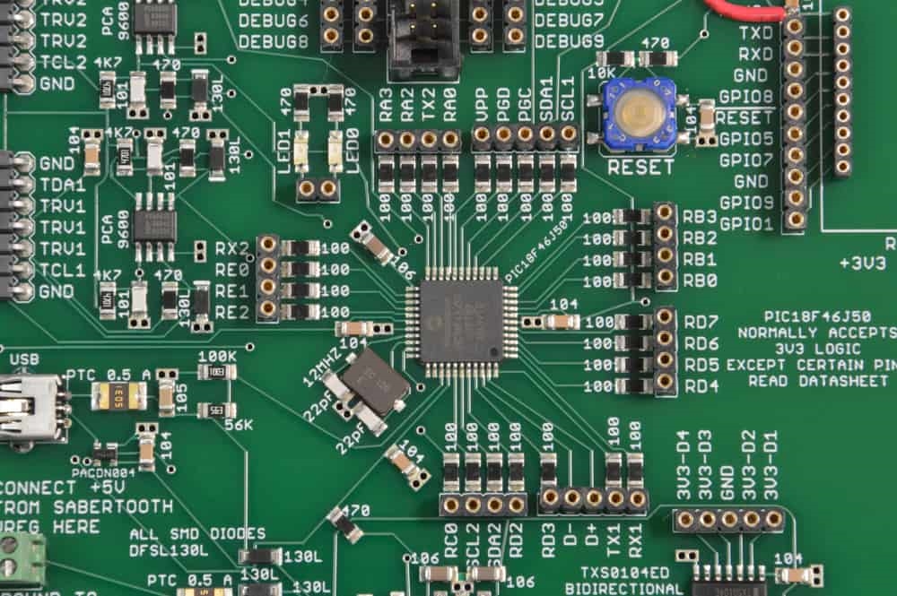
SMT assembly involves mounting electronic components directly onto the surface of a printed circuit board, unlike traditional through-hole methods that require drilling holes. This technology enables smaller board sizes, faster assembly, and higher component density, making it ideal for modern devices like smartphones and medical equipment. For electrical engineers, SMT matters because it directly impacts production speed and product reliability. A PCB design not optimized for SMT can lead to issues like misalignment, soldering defects, or thermal stress during reflow. These problems can delay projects and increase costs. By prioritizing PCB design for SMT assembly, engineers ensure smoother manufacturing, better yield rates, and consistent quality. Ultimately, optimizing for SMT is not just a design choice but a strategic step to meet industry demands for efficiency and innovation.
Technical Principles of PCB Design for SMT Assembly
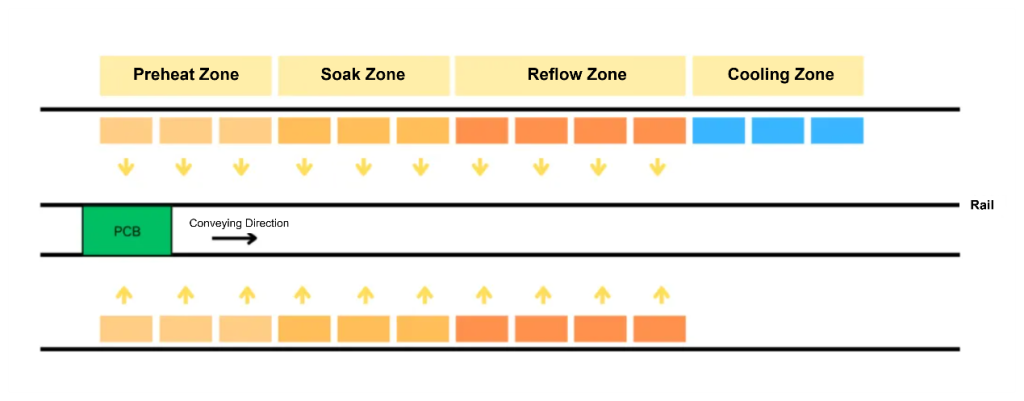
To optimize PCB design for SMT, engineers must understand the core principles that govern component placement, board layout, and thermal management. SMT components, such as resistors, capacitors, and integrated circuits, rely on precise soldering to pads on the PCB surface. This requires careful attention to pad dimensions, spacing, and orientation to avoid defects like tombstoning or bridging during reflow soldering.
One key principle is maintaining uniform thermal distribution across the board. Uneven heat during reflow can cause components to shift or fail to bond properly. Copper balancing, achieved by distributing copper evenly on both sides of the PCB, helps manage thermal stress. Another critical factor is ensuring adequate spacing between components to allow for accurate pick-and-place operations and to prevent solder joint interference.
Additionally, the design must account for the reflow soldering process, where components are subjected to high temperatures. Selecting materials and finishes that withstand these conditions, while adhering to industry standards, is vital for reliability. Standards like IPC-7351B provide guidelines for land pattern design, ensuring compatibility with SMT assembly equipment and processes.
Related Reading: Mastering PCB Assembly: A Comprehensive Guide to Surface Mount Technology
Best Practices to Optimize PCB Design for SMT Assembly
Optimizing a PCB design for SMT assembly involves actionable steps that align with manufacturing capabilities and quality requirements. Below are practical guidelines to enhance your design process.
Component Placement Strategies
Place components logically to minimize assembly errors. Group similar components together and orient them in the same direction to streamline pick-and-place operations. Ensure sufficient spacing between components, following recommendations from standards like IPC-7351B, to avoid interference during soldering. Position larger or heavier components centrally to balance the board and reduce the risk of warpage during reflow.
Pad Design and Solder Mask Precision
Accurate pad design is crucial for reliable SMT assembly. Follow land pattern guidelines from IPC-7351B to match pad sizes and shapes to component specifications. Avoid excessive solder mask clearance, as it can lead to solder bridging. Define solder mask openings precisely to expose only the necessary pad area, ensuring clean solder joints.
Via Placement and Routing Considerations
Avoid placing vias under SMT components, as they can interfere with soldering or cause uneven surfaces. If unavoidable, ensure vias are tented or filled to prevent solder wicking. Route traces efficiently to reduce signal interference and maintain a clear path for assembly equipment. Keep high-speed signals away from SMT pads to minimize noise.
Panelization for Efficient Assembly
Design your PCB with panelization in mind to facilitate mass production. Include fiducial marks for alignment during SMT assembly, adhering to guidelines in IPC-6012E for manufacturing compatibility. Add breakaway tabs or V-scoring to allow easy separation of individual boards without damaging components.
Thermal Management Techniques
Incorporate thermal relief patterns for large ground planes to prevent heat dissipation issues during soldering. Balance copper distribution on all layers to avoid uneven heating, which can cause board warpage. Standards like IPC-2221B offer detailed advice on managing thermal aspects in PCB design for SMT processes.
Common Challenges in SMT Assembly and How to Address Them
Even with a well-planned PCB design, SMT assembly can present challenges that affect yield and reliability. One frequent issue is component misalignment during pick-and-place, often due to inaccurate fiducial marks or poor pad design. To mitigate this, ensure fiducial marks are placed according to IPC-6012E and verify pad dimensions against IPC-7351B standards.
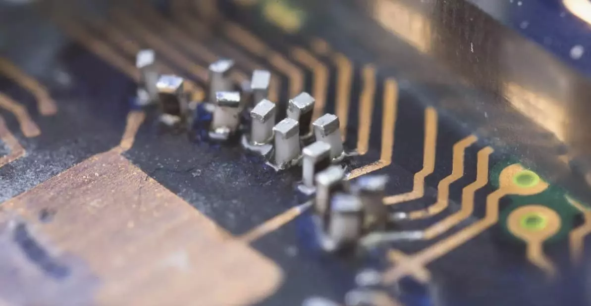
Another challenge is tombstoning, where small components lift on one end during reflow. This can result from uneven pad sizes or thermal imbalance. Correct this by ensuring symmetrical pad designs and balancing copper layers as recommended in IPC-2221B. Solder bridging, caused by excessive solder or tight spacing, can be prevented by adhering to spacing guidelines and optimizing stencil design per IPC-7525B.
Warpage during reflow is also a concern, especially for thin or large boards. Address this by selecting materials with appropriate thermal stability and designing for uniform copper distribution. Following IPC-A-600K for board acceptability criteria helps identify potential warpage risks early in the design phase.
Related Reading: Prevent SMT Soldering Defects: Tips
Tools and Standards for SMT-Optimized PCB Design
Leveraging industry standards is essential for creating PCB designs that align with SMT assembly requirements. The IPC-7351B standard provides detailed specifications for land patterns, ensuring components fit precisely on pads during assembly. Similarly, IPC-6012E outlines performance and qualification criteria for rigid boards, guiding engineers in material selection and layout planning.
For solder stencil design, IPC-7525B offers best practices to achieve uniform solder paste application, a critical factor in SMT soldering quality. Additionally, IPC-A-600K sets acceptability criteria for finished boards, helping designers identify and correct issues before manufacturing. Adhering to ISO 9001:2015 for quality management ensures that the design process remains consistent and traceable, reducing errors in SMT assembly.
Beyond standards, simulation tools can predict thermal behavior and signal integrity, allowing engineers to refine their PCB design before fabrication. These tools, combined with strict adherence to recognized guidelines, create a robust framework for SMT optimization.
Conclusion
Optimizing PCB design for SMT assembly is a fundamental aspect of modern electronics engineering. By focusing on precise component placement, accurate pad design, and thermal management, engineers can significantly enhance assembly efficiency and product reliability. Adhering to industry standards such as IPC-7351B and IPC-6012E ensures compatibility with manufacturing processes, reducing the risk of defects like tombstoning or warpage. Implementing the best practices outlined in this guide allows for smoother transitions from design to production, saving time and resources. As SMT technology continues to evolve, staying aligned with proven guidelines and continuously refining PCB design approaches will remain critical for achieving high-quality outcomes in electronics manufacturing.
FAQs
Q1: How does PCB design impact SMT assembly efficiency?
A1: PCB design directly affects SMT assembly efficiency by determining component placement accuracy and soldering quality. A well-optimized layout with proper spacing and fiducial marks, as per IPC-6012E, ensures precise pick-and-place operations. This reduces errors, speeds up assembly, and improves yield. Poor design can lead to misalignment or defects, slowing down production and increasing costs for engineers.
Q2: What are key factors to optimize in PCB design for SMT?
A2: To optimize PCB design for SMT, focus on component orientation, pad sizing per IPC-7351B, and thermal balance. Ensure adequate spacing to prevent solder bridging and use fiducial marks for alignment. Balanced copper distribution minimizes warpage during reflow. Following these steps ensures compatibility with assembly equipment and enhances reliability during manufacturing.
Q3: Why is thermal management important in SMT PCB design?
A3: Thermal management in SMT PCB design prevents warpage and soldering defects during reflow. Uneven heat distribution can shift components or weaken joints. Using thermal relief patterns and balancing copper layers, as guided by IPC-2221B, ensures uniform heating. This protects component integrity and maintains board stability, critical for reliable assembly outcomes.
Q4: How do industry standards help in optimizing SMT assembly?
A4: Industry standards like IPC-7351B and IPC-6012E provide proven guidelines for land patterns and board performance in SMT assembly. They ensure designs match manufacturing capabilities, reducing errors like misalignment or poor soldering. Adhering to ISO 9001:2015 maintains process consistency. Standards help engineers create reliable, high-quality PCBs tailored for efficient production.
References
IPC-7351B - Generic Requirements for Surface Mount Design and Land Pattern Standard. IPC, 2010.
IPC-6012E - Qualification and Performance Specification for Rigid Printed Boards. IPC, 2020.
IPC-2221B - Generic Standard on Printed Board Design. IPC, 2012.
IPC-7525B - Stencil Design Guidelines. IPC, 2011.
IPC-A-600K - Acceptability of Printed Boards. IPC, 2020.
ISO 9001:2015 - Quality Management Systems. ISO, 2015.


