Introduction
Thermal management remains a critical concern in PCB prototyping, especially as electronic devices become smaller and more powerful. Excessive heat can degrade component performance, reduce lifespan, and cause system failures. For electrical engineers, addressing heat dissipation during the early stages of design is vital to ensure reliability and functionality. This article explores the core challenges of PCB thermal management and offers practical techniques for effective heat dissipation. From thermal via placement to heat sink design for PCBs, the focus is on actionable strategies that align with industry standards. Whether working on high-power PCB designs or compact prototypes, understanding and applying PCB cooling techniques can significantly enhance project outcomes. Let’s dive into the principles and solutions that drive successful thermal management.
Why Thermal Management Matters in PCB Prototyping
In PCB prototyping, thermal management directly impacts the performance and durability of electronic systems. As components like microprocessors and power transistors generate heat during operation, the risk of thermal stress increases. Elevated temperatures can lead to solder joint failures, component degradation, and unexpected behavior in high-power PCB designs. Poor heat dissipation also affects signal integrity and may cause electromagnetic interference. For engineers, early consideration of PCB thermal management prevents costly redesigns and ensures prototypes meet operational requirements. With the trend toward miniaturization, managing heat in confined spaces becomes even more challenging. Effective strategies not only protect components but also maintain system efficiency, making thermal management a cornerstone of reliable PCB design.
Technical Principles of Heat Generation in PCBs
Understanding the sources and mechanisms of heat generation is the first step in addressing thermal challenges. Heat in PCBs primarily arises from power dissipation in active components such as integrated circuits and transistors. Resistive losses in copper traces and solder joints also contribute to temperature rise. The thermal conductivity of materials used in the board plays a significant role in how heat spreads or accumulates. For instance, standard FR-4 substrates have lower thermal conductivity compared to advanced materials, often leading to localized hot spots in high-power PCB designs.
Heat transfer occurs through conduction, convection, and radiation. Conduction moves heat through the board and components, while convection dissipates it into the surrounding air. Radiation, though less significant, transfers heat via electromagnetic waves. Inadequate airflow or poor material choices can trap heat, exacerbating thermal issues. Engineers must analyze these mechanisms during prototyping to predict and mitigate potential problems. Standards like IPC-2152, which provides guidelines for current-carrying capacity and temperature rise in traces, offer valuable benchmarks for thermal analysis during design.
Common Thermal Challenges in PCB Prototyping
Prototyping often reveals thermal issues that are harder to predict in simulations. One frequent challenge is uneven heat distribution, where certain areas of the board experience higher temperatures due to component density. This is common in compact designs with limited space for PCB cooling techniques. Another issue is insufficient thermal pathways, especially when relying on standard substrates without enhanced heat dissipation features.
High-power PCB designs face additional hurdles, as components like power amplifiers generate significant heat in short bursts. Without proper thermal via placement or heat sink design for PCBs, these components risk overheating. Environmental factors, such as ambient temperature and enclosure design, further complicate heat management. Addressing these challenges requires a combination of material selection, layout optimization, and strategic use of cooling methods, all while adhering to industry standards like IPC-2221B for generic PCB design and thermal considerations.
Practical Solutions for Heat Dissipation in PCB Prototyping
Optimizing Thermal Via Placement
Thermal vias are small conductive pathways that transfer heat from one layer of the PCB to another, often to a ground plane or heat sink. Proper thermal via placement is crucial for effective heat dissipation. Place vias directly beneath or near heat-generating components to create a short path for heat to escape. The density and size of vias should align with the expected thermal load, ensuring they do not compromise structural integrity or electrical performance. Following guidelines from IPC-6012E, which covers qualification and performance of rigid boards, ensures vias are implemented correctly for thermal and mechanical reliability.
Related Reading: Enhancing PCB Reliability: A Guide to Thermal Vias for Heat Dissipation
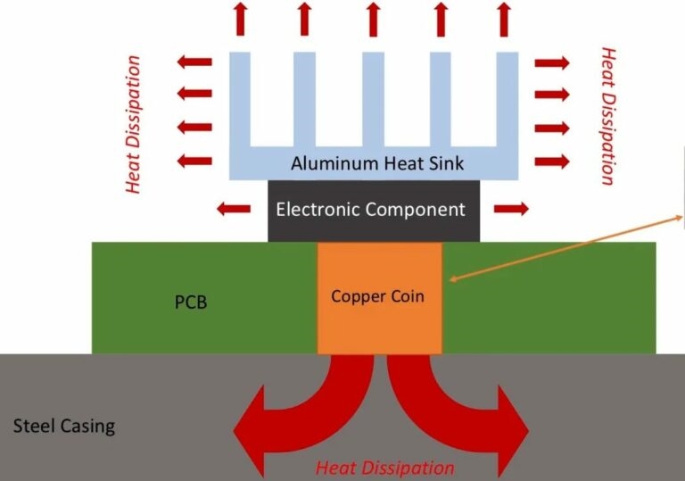
Heat Sink Design for PCBs
Incorporating heat sinks is a proven method for managing heat in high-power PCB designs. Heat sinks increase the surface area available for convection, allowing heat to dissipate into the surrounding environment. When designing a heat sink for a PCB, consider the material, typically aluminum or copper, based on thermal conductivity and weight constraints. Position the heat sink close to the heat source, ensuring secure mounting to maximize contact and heat transfer. Fin geometry and orientation should facilitate airflow, whether natural or forced, to enhance cooling efficiency.
Material Selection for Enhanced Thermal Conductivity
The choice of substrate material significantly impacts PCB thermal management. Standard FR-4 materials may suffice for low-power designs but often fall short in high-heat scenarios. Consider using substrates with higher thermal conductivity, such as metal-core or ceramic-based materials, for better heat spreading. These materials, while more expensive, reduce the risk of hot spots and improve overall performance. Refer to IPC-4101E for specifications on laminate materials to ensure compatibility with thermal and electrical requirements during prototyping.
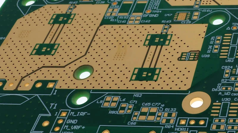
Layout Strategies for PCB Cooling Techniques
Board layout plays a pivotal role in heat dissipation. Spread heat-generating components across the board to avoid concentrated hot spots. Place sensitive components away from high-heat areas to protect their functionality. Use copper pours or planes as thermal conductors to distribute heat evenly across the PCB. Increasing trace width for high-current paths also reduces resistive heating, aligning with recommendations in IPC-2152 for safe temperature limits. Additionally, ensure adequate spacing for airflow if using passive cooling methods.
Active and Passive Cooling Methods
Cooling techniques for PCBs can be passive or active. Passive methods, like heat sinks and thermal vias, rely on natural convection and conduction without moving parts. Active cooling, such as fans or liquid cooling systems, introduces forced convection to remove heat more rapidly. For prototyping, passive methods are often preferred due to simplicity and cost. However, in high-power PCB designs, active cooling may be necessary to maintain safe operating temperatures. Evaluate the trade-offs between complexity and performance when selecting a cooling approach.
Advanced Strategies for High-Power PCB Design
High-power PCB designs demand specialized techniques to handle intense thermal loads. One approach is embedding thermal management features directly into the board structure. For instance, integrating metal cores or heat pipes within multilayer boards can significantly enhance heat dissipation. These solutions require careful planning during the design phase to ensure compatibility with other board elements.
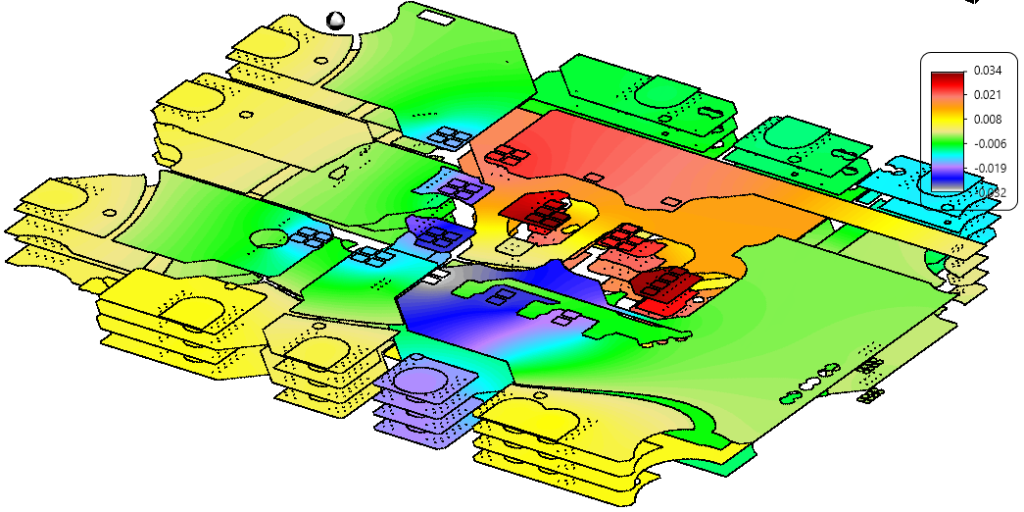
Another strategy involves using simulation tools to predict thermal behavior before prototyping. Thermal analysis software helps identify potential hot spots and evaluate the effectiveness of proposed cooling methods. Standards like IPC-2221B provide a framework for incorporating thermal design considerations, ensuring that high-power designs remain within safe operating limits. Combining simulation with physical testing during prototyping offers a comprehensive approach to tackling thermal challenges.
Related Reading: Thermal PCB design
Troubleshooting Thermal Issues in Prototyping
During PCB prototyping, thermal issues may surface despite careful planning. If components overheat, first check the placement of thermal vias and ensure they align with heat sources. Verify that copper planes are adequately sized and connected to dissipate heat. If using a heat sink, confirm proper contact with the component surface to minimize thermal resistance. Ambient conditions, such as enclosure design, should also be assessed for their impact on airflow.
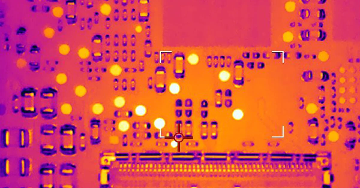
Testing with thermal imaging tools can pinpoint problem areas, allowing for targeted adjustments. If issues persist, consider revising the board layout or upgrading to materials with better thermal properties. Documenting these findings during prototyping helps refine future designs and prevents recurring thermal problems. Adhering to IPC-A-600K for acceptability of printed boards ensures that troubleshooting efforts meet industry quality standards.
Conclusion
Thermal management is a cornerstone of successful PCB prototyping, particularly as designs grow more complex and power-intensive. By understanding the principles of heat generation and applying practical solutions like thermal via placement, heat sink design for PCBs, and optimized layouts, engineers can mitigate thermal challenges effectively. High-power PCB designs benefit from advanced strategies and thorough testing to ensure reliability. Incorporating PCB cooling techniques early in the prototyping phase saves time and resources while enhancing performance. With guidance from established standards, such as those from IPC, electrical engineers can build prototypes that withstand thermal stress and deliver consistent results in real-world applications.
FAQs
Q1: How does thermal via placement improve PCB thermal management?
A1: Thermal vias create conductive paths to transfer heat away from components to other layers or heat sinks. Placing them near heat sources ensures efficient dissipation, reducing hot spots. Their design must balance thermal needs with electrical constraints, following industry standards for optimal performance in PCB thermal management.
Q2: What factors should be considered in heat sink design for PCBs?
A2: Heat sink design for PCBs requires selecting materials with high thermal conductivity, like aluminum or copper. Fin geometry and orientation must support airflow, while placement should ensure direct contact with heat-generating components. Weight and space constraints also influence the design for effective cooling.
Q3: Why is material selection critical in high-power PCB design?
A3: In high-power PCB design, materials with high thermal conductivity, like metal-core substrates, prevent overheating by spreading heat evenly. Standard materials may fail under intense loads, leading to component damage. Choosing the right substrate ensures reliability and aligns with thermal performance requirements.
Q4: What are effective PCB cooling techniques for compact prototypes?
A4: For compact prototypes, PCB cooling techniques include using thermal vias, copper pours, and small heat sinks for passive dissipation. Optimizing component spacing improves airflow, while high-conductivity materials enhance heat spread. These methods address space limitations while maintaining thermal stability in tight designs.
References
IPC-2152 — Standard for Determining Current Carrying Capacity in Printed Board Design. IPC, 2009.
IPC-2221B — Generic Standard on Printed Board Design. IPC, 2012.
IPC-6012E — Qualification and Performance Specification for Rigid Printed Boards. IPC, 2020.
IPC-4101E — Specification for Base Materials for Rigid and Multilayer Printed Boards. IPC, 2017.
IPC-A-600K — Acceptability of Printed Boards. IPC, 2020.


