Introduction
Printed circuit boards form the backbone of electronic devices, yet their lifespan often falls short due to design choices that complicate repairs. When components become inaccessible or the board warps under thermal stress, replacement becomes the default, driving up costs and contributing to electronic waste. Design for repairability shifts this paradigm by prioritizing serviceability from the initial layout stage. Engineers can extend PCB lifespan significantly while reducing long-term ownership expenses through strategic decisions in layout, materials, and testing features. This approach aligns with growing demands for sustainable electronics, where repairable designs minimize resource consumption. By focusing on design for repairability guidelines, teams achieve reliable performance over extended periods.
What Is Design for Repairability and Why It Matters
Design for repairability refers to intentional engineering practices that facilitate maintenance, component replacement, and fault isolation without excessive damage to the board. Core elements include accessible component placement, robust material selection, and built-in diagnostics. This methodology contrasts with cost-optimized designs that prioritize density over serviceability, often leading to premature failure. In high-reliability applications, such as industrial controls or medical devices, repairability directly impacts operational uptime and total cost of ownership. Poorly repairable PCBs result in higher downtime, labor-intensive fixes, and frequent full replacements. Embracing these principles supports compliance with quality standards and enhances product value.
The relevance intensifies in sectors facing regulatory pressure for sustainability. Repairable designs reduce landfill contributions from obsolete electronics. Economically, they lower warranty claims and extend service intervals, yielding savings that outweigh initial material costs. For electric engineers, integrating repairability early prevents downstream issues like solder joint fatigue from repeated rework attempts. Ultimately, it fosters a lifecycle approach where PCBs endure multiple interventions.
Key Technical Principles of Repairable PCB Design
Effective repairability hinges on understanding mechanical, thermal, and electrical stressors that degrade PCBs over time. Component placement for easy access ensures technicians can reach connectors, fuses, and ICs without desoldering adjacent parts. Crowded layouts amplify risks during soldering, increasing defect rates. Durable materials resist delamination and cracking, preserving integrity through thermal cycles. Thermal stress minimization prevents warpage, which obstructs probe access and compromises traces.

Mechanical durability starts with substrate choices that maintain dimensional stability. High glass transition temperature materials withstand repeated heating without bowing. Trace routing avoids sharp bends near high-stress zones, reducing fracture propensity. These principles interlink; for instance, improper heat dissipation accelerates material fatigue, complicating future repairs.
Thermal management principles address coefficient of thermal expansion mismatches between components and the board. Excessive gradients cause microcracks in solder joints, rendering areas irreparable. Conformal coatings protect against environmental ingress but must allow rework without residue buildup. Adhering to JEDEC standards for moisture sensitivity aids in maintaining repair windows post-storage.
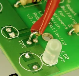
Component Placement for Easy Access
Strategic component placement forms the foundation of design for repairability guidelines. Grouping similar functions into modular zones simplifies isolation during faults. Tall components like electrolytic capacitors position away from dense BGA areas to avoid shadowing during reflow or rework. Fiducial marks near critical sections guide automated tools precisely. Edge connectors and test points cluster for quick diagnostics, minimizing handling time.
This layout reduces cross-contamination risks from flux vapors in soldering irons. Symmetrical placement balances mechanical loads, preventing warpage that hinders probe insertion. For multilayer boards, via-in-pad avoidance near repair zones preserves flatness. Engineers benefit from simulations verifying access paths before fabrication.
Selecting Durable PCB Materials
Selecting durable PCB materials enhances resistance to repeated repairs. Laminates with high thermal decomposition temperatures endure multiple rework cycles without charring. Low moisture absorption prevents popcorning during desoldering, a common failure mode. Copper foil weights balance conductivity and etch tolerance for trace repairs.
Material stackups influence overall robustness; thicker cores distribute stress evenly. Surface finishes like ENIG support multiple soldering events without pad lifting. Compliance with IPC-4101 specifications ensures consistency in these properties. Such choices extend lifespan by mitigating degradation from handling.
Minimizing Thermal Stress in PCB Design
Minimizing thermal stress in PCB design involves vias for heat spreading and copper planes for dissipation. Thermal vias under power devices channel heat away, preventing localized hotspots that embrittle nearby components. Slotting ground planes reduces thermal mass imbalances across layers. Simulations predict stress concentrations, guiding layout adjustments.
Component orientation aligns heat sources with airflow paths in enclosures. Keep-out zones around high-power ICs prevent thermal coupling to sensitive analog sections. These measures preserve solder joint integrity, crucial for repair success. Per IPC-6012 guidelines, controlled impedance traces avoid signal distortion from thermal expansion.
Designing PCBs for Easy Troubleshooting
Designing PCBs for easy troubleshooting incorporates boundary scan chains and embedded test points. Daisy-chained JTAG ports enable in-circuit programming without full disassembly. Voltage monitoring pads at power rails facilitate quick fault checks. Silkscreen labels with reference designators speed visual inspection.
Built-in self-test circuits detect opens and shorts pre-failure. Redundant traces in critical paths allow rerouting during repairs. These features cut diagnostic time, preserving board life. Logical partitioning into functional blocks isolates issues efficiently.
Best Practices and Implementation Strategies
Follow design for repairability guidelines by starting with a serviceability checklist during schematic capture. Prioritize through-hole for high-failure components amenable to hand replacement. Standardize footprints across families for tool compatibility. Prototype testing validates access under fatigue simulations.
Collaborate with assembly teams for feedback on rework feasibility. Document repair procedures tied to the layout. Iterate based on field returns, refining placement iteratively. These practices yield measurable lifespan extensions.
Conclusion
Design for repairability profoundly influences PCB lifespan and cost by embedding serviceability into core engineering decisions. Component placement for easy access, durable materials, thermal stress minimization, and troubleshooting features collectively reduce failure cascades. Electric engineers adopting these strategies achieve resilient designs compliant with industry benchmarks. Long-term benefits include cost efficiencies and sustainability gains. Prioritizing repairability transforms PCBs from disposable to durable assets.
FAQs
Q1: What are key design for repairability guidelines for PCBs?
A1: Design for repairability guidelines emphasize modular layouts, accessible test points, and robust materials. Place high-maintenance components near edges, incorporate thermal vias, and use durable laminates per IPC standards. These practices simplify fault isolation and replacement, extending board life while cutting repair costs. Logical structuring ensures compliance and repeatability.
Q2: How does component placement for easy access impact PCB repairs?
A2: Component placement for easy access groups functions modularly and avoids dense clustering around critical parts. This allows precise desoldering without damaging neighbors, reducing rework time. Fiducials and edge connectors further aid tool alignment. Resulting designs support multiple service cycles, lowering total ownership expenses.
Q3: Why is minimizing thermal stress in PCB design essential for repairability?
A3: Minimizing thermal stress in PCB design prevents warpage and joint fatigue that obstruct repairs. Thermal vias and balanced planes distribute heat evenly, preserving flatness. Materials with matched expansion coefficients avoid cracks. This maintains accessibility over time, aligning with JEDEC moisture handling for sustained performance.
Q4: What role does selecting durable PCB materials play in troubleshooting?
A4: Selecting durable PCB materials resists degradation from repeated handling and heating. High-Tg laminates and reliable finishes endure desoldering without lifting. Low-hygroscopic properties prevent defects during storage. These choices facilitate designing PCBs for easy troubleshooting, minimizing downtime in field applications.
References
IPC-4101E — Specification for Base Materials for Rigid and Multilayer Printed Boards. IPC, 2017
IPC-6012E — Qualification and Performance Specification for Rigid Printed Boards. IPC, 2018
JEDEC J-STD-020E — Moisture/Reflow Sensitivity Classification of Nonhermetic Surface Mount Devices. JEDEC, 2014