Introduction
Metal core printed circuit boards represent a specialized solution for applications demanding superior thermal performance, such as power electronics, LED lighting, and automotive systems. Unlike standard FR-4 boards, metal core PCBs incorporate a thick metal substrate, typically aluminum or copper, to efficiently dissipate heat generated by high-power components. The PCB stackup, or layer arrangement, plays a pivotal role in balancing thermal management, signal integrity, and mechanical stability. Proper design ensures reliable operation under elevated temperatures while maintaining controlled impedance for high-frequency signals. This guide explores the fundamentals of metal core PCB stackup design, offering electric engineers structured insights into optimizing layer configurations for real-world challenges. By understanding these principles, designers can enhance board reliability and performance.
What Is a Metal Core PCB Stackup and Why It Matters
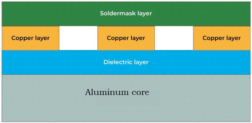
A metal core PCB stackup refers to the precise sequence and thickness of materials layered together to form the board, with the metal core serving as the foundational heat-spreading element. This arrangement typically includes one or two copper circuit layers separated from the core by a thin, thermally conductive dielectric layer. The core itself provides structural rigidity and a low-thermal-resistance path to external heatsinks. In high-power density designs, effective PCB stackup prevents hotspots that could degrade components or cause failures. For electric engineers, mastering layer arrangement directly impacts thermal management and signal integrity, ensuring compliance with performance expectations. Poor stackup choices lead to issues like delamination or excessive warpage during thermal cycling.
The relevance of metal core PCB stackups stems from their ability to handle power levels far beyond conventional multilayers. Standard PCBs rely on thin copper planes for heat spreading, but metal cores offer conductivities orders of magnitude higher. This makes them essential in environments where junction temperatures exceed 100 degrees Celsius. Engineers must consider the interplay between electrical isolation, heat transfer, and mechanical stress when defining the stackup. Optimized designs reduce overall system costs by minimizing the need for additional cooling solutions.
Key Components of Metal Core PCB Layer Arrangement
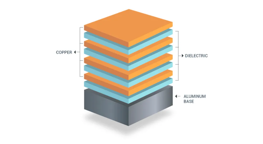
The foundational layer in any metal core PCB stackup is the metal substrate, usually 1 to 2 mm thick, which acts as both a mechanical base and thermal conductor. Above this sits the dielectric insulator, a critical thin layer of ceramic-filled polymer, often 75 to 150 micrometers thick, that bonds the core to the copper circuit layer while providing electrical isolation. Copper traces, typically 1 to 3 ounces per square foot, form the signal or power paths on the top surface, with solder mask completing the outer layer. In double-sided configurations, a second copper layer mirrors the top, separated by another dielectric sheet. For multilayer metal core PCBs, additional signal layers stack above the first copper plane using prepregs, but the core remains at the base to maximize heat extraction. This layer arrangement demands careful material selection to match coefficients of thermal expansion and avoid stress concentrations.
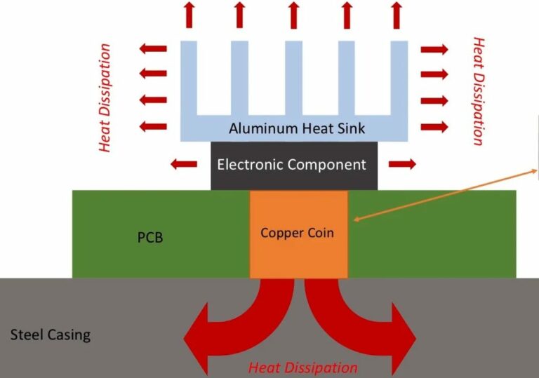
Engineers must account for via structures within the stackup, as thermal vias transfer heat from components directly to the core. Filled or blind vias prevent exposure of the core, maintaining isolation. The positioning of ground planes influences return paths and shielding. Asymmetric builds require compensation to prevent warpage, aligning with general principles in IPC-2221 for printed board design. Each component contributes to the overall thermal and electrical performance of the board.
Thermal Management Principles in Metal Core PCB Stackups
Thermal management begins with selecting a dielectric material boasting high thermal conductivity, typically 1 to 4 W/mK, far superior to standard epoxy. The thin dielectric minimizes thermal resistance between heat-generating traces and the core, enabling rapid heat spreading. In stackup design, placing high-power components over areas with dense via fields ensures efficient conduction to the core. The metal substrate then dissipates heat laterally or to an attached heatsink. Simulations reveal that optimal layer thicknesses reduce peak temperatures by channeling heat away from sensitive areas. Electric engineers prioritize this in stackups to extend component lifetimes and maintain operational margins.
Layer arrangement further enhances thermal paths by incorporating embedded ground planes that double as heat spreaders. Vias arrayed in patterns, such as 0.3 mm diameter on 0.8 mm pitch, bridge upper layers to the core without compromising isolation. Core thickness influences spreading effectiveness; thicker cores excel in uniform dissipation but add weight. Balancing these elements prevents thermal runaway in dense power layouts. Adhering to thermal design guidelines in IPC-2221 helps predict and mitigate hotspots during operation.
Impedance Control in Metal Core PCB Designs
Impedance control proves challenging in metal core PCBs due to the thin dielectric and proximity of the conductive core, which alters field distributions. Traces on the top copper layer behave as microstrips referenced to the core through the dielectric, requiring wider widths for target impedances like 50 ohms. Designers calculate effective dielectric constants considering the core's influence, often using field solver approximations. Layer arrangement affects this; additional ground planes above the first signal layer stabilize reference planes for striplines. Maintaining tolerances within 10% demands precise control of dielectric thickness and copper roughness. Signal integrity benefits from consistent impedance, reducing reflections in high-speed interfaces.
For multilayer stackups, interleaving signal and plane layers minimizes loop inductance. Edge effects near board edges necessitate guard traces or stitching vias to the core. Copper weight selection impacts skin effect losses at frequencies above 1 GHz. Engineers iterate stackups to achieve both thermal management and impedance targets simultaneously.
Signal Integrity Considerations for Metal Core PCB Stackups
Signal integrity in metal core PCBs hinges on robust return paths and minimized crosstalk, facilitated by the core as a solid ground reference. The stackup's ground plane placement shields sensitive traces from external interference while providing low-impedance returns. In high-frequency applications, the thin top dielectric increases capacitive coupling to the core, demanding careful trace spacing per general design rules. Vias introduce discontinuities; tenting or filling them preserves integrity. Layer arrangement with symmetric builds reduces skew between differential pairs. Electric engineers verify these through time-domain reflectometry simulations tailored to the stackup.
Crosstalk mitigation involves solid pours connected to the core via extensive stitching. Power integrity ties into this, as the core distributes plane currents effectively. Thermal expansion mismatches can warp traces over cycles, degrading signals; thus, CTE-matched materials are essential. Optimizing the PCB stackup ensures clean eye diagrams even under thermal stress.
Best Practices for Metal Core PCB Stackup Design
Start stackup design by defining thermal requirements, selecting core thickness based on power dissipation needs. Use the thinnest viable dielectric to lower thermal resistance without risking breakdown voltage. For multilayers, limit to four or six layers to avoid excessive asymmetry, placing the core at the bottom for direct heatsink attachment. Incorporate thermal reliefs on pads connected to the core to ease soldering while preserving conduction. Simulate the full stackup for warpage using finite element analysis, compensating with balanced copper distribution. Document the layer arrangement with detailed fab drawings specifying material specs and tolerances.
Impedance control best practices include referencing all critical traces to planes tied to the core. Array thermal vias under hot components, filling with conductive epoxy for multilayers. Avoid routing high-speed signals over large core cutouts, as they disrupt references. Per IPC-6012 performance specifications, ensure via plating integrity to prevent delamination. Prototype and test stackups for real-world validation.
Common Challenges and Troubleshooting in Stackup Design
Warpage emerges as a primary challenge in metal core PCB stackups due to CTE mismatches between the core and organic layers. Asymmetric builds exacerbate this during reflow or operation; symmetric layering or counterbalancing copper pours mitigates it. Delamination at the dielectric-core interface arises from poor adhesion or moisture; prebaking and plasma treatment resolve this. Impedance variations from dielectric inconsistencies require statistical process controls. Thermal vias plugging during plating demands larger antipads. Troubleshooting involves sectioning prototypes and microscopy per IPC-A-600 acceptability criteria.
Signal reflections from via stubs in multilayers call for back-drilling or blind vias. Hotspot persistence indicates insufficient via density; redesign arrays iteratively. Mechanical stress cracking traces necessitates wider bends and reliefs.
Conclusion
Mastering metal core PCB stackup design equips electric engineers to tackle thermal management, impedance control, and signal integrity in demanding applications. Key principles revolve around thin dielectrics for heat transfer, solid core referencing for electrical performance, and balanced layer arrangements for reliability. Best practices like via optimization and simulations yield robust boards. By applying structured approaches, designers achieve efficient power handling without compromising functionality. This foundational knowledge supports innovation in high-reliability electronics.
FAQs
Q1: What role does layer arrangement play in thermal management for metal core PCBs?
A1: Layer arrangement positions the metal core directly beneath heat sources via thin dielectrics, minimizing thermal resistance. Thermal vias bridge upper layers to the core, spreading heat laterally. Balanced stackups prevent hotspots, ensuring uniform dissipation. This setup outperforms standard PCBs in high-power scenarios, aligning with design guidelines for longevity.
Q2: How do you achieve impedance control in a metal core PCB stackup?
A2: Impedance control relies on precise dielectric thickness and trace geometry, accounting for core proximity in microstrip configurations. Wider traces compensate for lower heights, maintaining 50-ohm targets. Ground stitching stabilizes references. Simulations verify tolerances amid manufacturing variations, preserving signal integrity.
Q3: Why is signal integrity critical in metal core PCB designs?
A3: Signal integrity ensures low reflections and crosstalk in high-speed signals over the unique stackup. The core provides excellent ground returns, but thin dielectrics heighten coupling risks. Proper plane placement and via management mitigate EMI. Optimized layer arrangement supports reliable data transmission under thermal loads.
Q4: What are common pitfalls in metal core PCB stackup layer arrangement?
A4: Common pitfalls include asymmetry causing warpage and inadequate via thermal paths leading to hotspots. Ignoring CTE mismatches risks delamination. Overlooking impedance shifts from core effects degrades signals. Address via balanced builds, simulations, and standards-compliant materials.
References
IPC-2221A — Generic Standard on Printed Board Design. IPC, 2003
IPC-6012E — Qualification and Performance Specification for Rigid Printed Boards. IPC, 2017
IPC-A-600K — Acceptability of Printed Boards. IPC, 2020


