Introduction
The relentless demand for smaller, more powerful electronic devices has placed unprecedented pressure on printed circuit board (PCB) designers to achieve higher component densities within constrained spaces. Stacked vias emerge as a pivotal technology in this landscape, enabling stacked via miniaturization by allowing multiple interlayer connections in a compact vertical column. Unlike traditional through-hole vias that traverse the entire board thickness, stacked vias utilize microvias aligned directly atop one another across sequential layers, maximizing routing efficiency in high-density PCBs. This approach is particularly vital for small form factor PCBs used in modern applications where every square millimeter counts. As engineers tackle the challenges of signal integrity and thermal management in denser layouts, understanding stacked vias becomes essential for pushing the boundaries of PCB performance. Their adoption marks a significant shift toward more efficient, reliable interconnects in advanced electronics.
What Are Stacked Vias and Why Do They Matter?
Stacked vias consist of multiple blind or buried microvias positioned directly on top of each other, forming a continuous conductive path through several layers without lateral offset. This configuration contrasts with staggered vias, where each via is slightly shifted to improve mechanical reliability but at the cost of additional board area. In high-density interconnect (HDI) PCBs, stacked vias facilitate stacked via space saving by minimizing the footprint required for interlayer transitions, which is crucial for achieving ultra-fine pitch component placement. Engineers specify them in designs targeting small form factor PCBs, such as those in wearables and IoT modules, where traditional via structures would consume excessive real estate.
The relevance of stacked vias stems from the industry's transition to finer feature sizes driven by Moore's Law extensions and consumer expectations for portability. They enable higher via densities, supporting ball grid array (BGA) packages with pitches below 0.5 mm and reducing overall board size by up to 30 percent in optimized stackups. Reliability concerns, however, necessitate careful design, as misalignment during lamination can compromise conductivity. For electric engineers, mastering stacked vias means balancing density gains against fabrication tolerances and material behaviors. Their integration aligns with the need for high-density PCBs in performance-critical sectors, revolutionizing how we approach miniaturization without sacrificing functionality.
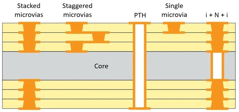
Stacked vs Staggered vs Skipped Vias: Pros, Cons, and When to Choose Each
Understanding the differences is critical before committing to a design. The table below summarizes the trade-offs.
| Via Type | Density Gain | Reliability | Manufacturing Complexity | Cost Premium | Best Applications | Key Limitation |
|---|---|---|---|---|---|---|
| Stacked | Highest (up to 30% smaller board) | Good when limited to 2–3 levels and filled | High (multiple plating cycles, tight registration) | 20–40% | Fine-pitch BGA fan-out, smartphones, wearables | Higher risk of cracking if >3 levels |
| Staggered | Medium | Highest (stress distributed) | Medium | 10–25% | Automotive, medical, high-reliability aerospace | Consumes more routing channels |
| Skipped | Lowest | Very High | Lowest | Baseline | Cost-sensitive, low-layer count designs | Largest footprint, limited density |
Decision Framework: Choose stacked vias when board real estate is the primary constraint and stack height can be limited to two or three levels. Opt for staggered vias in designs requiring maximum reliability under thermal cycling or vibration. Use skipped vias only when cost and simplicity outweigh density needs. In most modern HDI designs for consumer electronics, a hybrid approach—stacked in dense BGA areas and staggered elsewhere—delivers the best balance.
Technical Principles Behind Stacked Vias
At the core of stacked via functionality lies sequential lamination, a process where thin dielectric layers are added incrementally, allowing laser drilling of microvias with diameters typically under 100 microns. Each via is electroplated with copper to ensure low resistance and structural integrity, followed by precise alignment for the next layer buildup. The aspect ratio, defined as the depth-to-diameter ratio, must remain below 1:1 for reliable plating, as higher ratios risk voids or incomplete fills. In stacked configurations, cumulative stresses from thermal expansion mismatch between copper and dielectrics can induce microcracks, particularly during reflow soldering cycles. Reliable plating in these sequential builds often requires conductive or resin filling—see our in-depth guide on PCB microvia filling materials, methods, and reliability considerations.
Material selection plays a critical role, with low coefficient of thermal expansion (CTE) resins preferred to match the via barrel's properties and mitigate warpage. Per IPC-2226 guidelines for HDI design, via placement must account for drill registration tolerances, often limited to plus or minus 50 microns per layer. Signal integrity benefits from shorter via stubs, reducing inductance and enabling higher data rates in high-speed interfaces. Engineers model these structures using finite element analysis to predict electromigration and fatigue under operational loads. Overall, the principles ensure stacked vias support the electrical and mechanical demands of modern high-density PCBs.
Reliability testing focuses on thermal cycling and shock, where stacked vias demonstrate robustness when limited to two or three levels. Copper filling techniques, such as electroplating or conductive paste, enhance planarization and prevent resin voids during subsequent lamination. The vertical alignment demands advanced imaging, like automated optical inspection, to verify continuity across the stack.
Design and Manufacturing Best Practices for Stacked Vias
When designing with stacked vias, engineers should prioritize stackup planning to distribute vias evenly and avoid clustering that could exacerbate local heating. Adhere to minimum land sizes and annular rings as outlined in IPC-6012 for rigid board performance, ensuring at least 75 microns of copper around each via pad. Prefer staggered arrangements where possible for better stress distribution, reserving stacked vias for unavoidable high-density zones like processor fanouts. Simulate via thermal resistance to confirm current carrying capacity, typically rated for 1-2 amps per via depending on plating thickness. These density gains are best realized within a complete layer configuration—explore proven configurations in our overview of HDI PCB stack up design for optimizing layer count and signal routing.
Manufacturing begins with laser ablation for precise microvia formation, followed by desmear to remove dielectric residue and promote adhesion. Sequential buildup requires multiple plating cycles, with intermediate inspections to catch alignment drifts early. To enhance stacked via space saving in small form factor PCBs, incorporate via-in-pad designs, tenting unused vias with solder mask per industry guidelines. Post-lamination, X-ray verification confirms fill quality and barrel integrity.
Best practices also include specifying build-up films with matched CTE to the core laminate, reducing bow and twist during processing. Limit stacked via depth to two levels in production environments to align with proven reliability data, transitioning to staggered for deeper connections. Electrical testing via flying probe ensures open-circuit detection in hidden structures. These steps collectively optimize stacked via miniaturization while upholding quality in high-density PCBs.
Reliability, Failure Modes, and Testing Standards
Reliability data from accelerated life testing shows that copper-filled stacked vias reliably survive 1,000–2,000 thermal cycles when limited to two or three levels. Beyond three levels, failure rates rise sharply due to cumulative CTE mismatch stress.
Common Failure Modes
- Via cratering or barrel cracking (most frequent at the knee of the via).
- Delamination at the via–dielectric interface.
- Plating voids leading to open circuits after reflow.
Standards to follow include IPC-6012 Class 3 for rigid boards and IPC-6018 for HDI. Testing typically involves thermal shock, highly accelerated life testing (HALT), and highly accelerated stress screening (HASS). X-ray inspection and cross-section analysis are essential for validating fill quality and registration in hidden structures.
Manufacturing Process and Cost Considerations
Manufacturing stacked vias begins with laser drilling of the microvias, followed by desmear, electroless copper seeding, and electrolytic plating. Each additional layer in the stack requires a full plating cycle, planarization, and inspection, driving cost premiums of 15–40% compared to staggered via designs.
Key process steps include plasma or chemical desmear for adhesion, vacuum lamination to minimize voids, and AOI/X-ray verification between build-up stages. In high-volume production, panel utilization and yield become critical cost drivers. While the upfront NRE for complex HDI stack-ups is higher, the per-unit savings from reduced layer count and smaller board size often deliver strong ROI above 5,000–10,000 units.
Applications in Mobile Devices and Beyond
In mobile devices, stacked vias excel by enabling stacked via in mobile devices layouts that accommodate dense processor and memory arrays within slim profiles. For instance, smartphone motherboards leverage 4-8 layer HDI stackups with stacked microvias to route signals under fine-pitch BGAs, preserving board area for antennas and batteries. Automotive electronics benefit similarly, packing ADAS sensors into compact modules resistant to vibration. For high-density smartphone and wearable layouts, combining stacked vias with via-in-pad techniques delivers maximum space savings—learn more in our guide to sequential lamination and via-in-pad for maximizing component density on HDI PCBs.
Reliability in these applications hinges on IPC-6018 qualification for HDI boards, which mandates accelerated life testing to validate via performance under combined mechanical and thermal stresses. Engineers troubleshoot common failures like via cratering by refining drill parameters and plating baths. Case insights reveal that copper-filled stacked vias outperform unfilled ones in high-current paths, minimizing electromigration risks.
2026 Trends: Advanced Laser Techniques, Embedded Components, and AI-Optimized Via Placement
Laser drilling technology continues to improve, with UV and CO₂ lasers achieving sub-30 µm vias at higher throughput. Embedded component technology is increasingly combined with stacked vias to create true 3D interconnects that further shrink module size.
AI-driven EDA tools now optimize via placement and stacking patterns automatically, balancing density, thermal performance, and reliability constraints in seconds rather than hours. These advancements are expected to make 4-level reliable stacked vias commercially viable by late 2026, opening new possibilities for ultra-compact 5G-A and AR/VR hardware.
Conclusion
Stacked vias fundamentally transform PCB miniaturization by delivering unparalleled density in high-density PCBs and small form factor designs. Their precise engineering addresses the trade-offs between space efficiency and reliability, guided by established standards and best practices. Electric engineers can harness this technology to meet shrinking form factors without compromising performance, particularly in demanding applications like mobile devices. As fabrication capabilities advance, stacked vias will continue to drive innovation, enabling the next generation of compact, high-performance electronics. Prioritizing design rigor ensures these structures deliver on their promise of revolutionizing interconnect strategies.
FAQs
Q1: What role do stacked vias play in high-density PCB design?
A1: Stacked vias enable stacked via miniaturization by vertically aligning microvias to connect multiple layers within a minimal footprint, ideal for high-density PCBs. They reduce routing congestion around components, supporting finer pitches and shorter signal paths. Design per IPC guidelines ensures alignment and plating quality, while limiting stacks to two levels enhances reliability. This makes them essential for engineers optimizing board real estate logically.
Q2: How do stacked vias contribute to small form factor PCB development?
A2: In small form factor PCBs, stacked via space saving allows tighter component placement by eliminating lateral offsets required in staggered vias. Engineers achieve this through sequential lamination and copper filling for planarity. Reliability improves with CTE-matched materials to prevent cracking during thermal cycles. Practical implementation focuses on simulation and testing for vibration-prone applications.
Q3: What are key challenges in using stacked vias in mobile devices?
A3: Stacked via in mobile devices face alignment precision and thermal stress issues due to thin profiles and reflow processes. Best practices include copper electroplating and X-ray inspection to verify integrity. Staggered alternatives offer better reliability for deeper stacks, but pure stacked designs excel in density. Engineers balance these by modeling stresses and adhering to HDI standards.
Q4: How can engineers ensure reliability of stacked vias?
A4: Reliability stems from limiting stacks to two microvias, using low-CTE dielectrics, and full copper filling. Follow IPC-6012 for plating thickness and annular ring specs to avoid voids. Thermal cycling tests validate performance, with staggered vias preferred for cost-sensitive designs. Structured design reviews catch issues early, ensuring robust high-density interconnects.
References
IPC-2226 — Design Standard for High Density Interconnect (HDI) Printed Boards. IPC.
IPC-6012 — Qualification and Performance Specification for Rigid Printed Boards. IPC.
IPC-6018 — Qualification and Performance Specification for High Density Interconnect (HDI) Printed Boards. IPC.


