Introduction
In the push for smaller, more powerful electronics, high-density interconnect (HDI) printed circuit boards (PCBs) have become essential for accommodating increasing component counts. Engineers face the challenge of fitting fine-pitch components like ball grid arrays (BGAs) and chip-scale packages (CSPs) into limited board real estate. Sequential lamination and via-in-pad technology emerge as critical processes to boost HDI PCB component density without compromising signal integrity or reliability. These methods allow vias to be embedded directly within component pads, freeing up surface area for more parts. As devices shrink, understanding these techniques ensures designs meet performance demands in applications from consumer gadgets to aerospace systems. This article explores how sequential lamination enables via-in-pad, along with practical manufacturing insights.
Understanding Via-in-Pad Technology
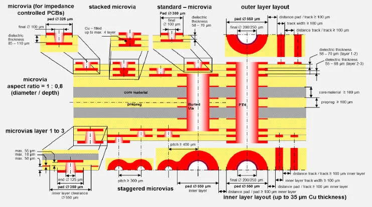
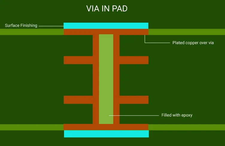
Via-in-pad technology involves placing microvias directly into the landing pads of surface-mount components, then filling and plating them to create a flat, solderable surface. This approach eliminates the need for larger fanout vias around pads, directly increasing available space for components. In HDI PCBs, where layer counts exceed six and microvias dominate interconnections, via-in-pad supports pitches below 0.4 mm. The result is higher routing density and shorter signal paths, which reduce inductance and improve electrical performance. Manufacturers must ensure the via fill material withstands thermal cycling and reflow soldering stresses. Proper implementation aligns with IPC-6012DS requirements for HDI board qualification. For a broader overview of microvia structures, see our complete guide to blind and buried vias in HDI PCBs.
Engineers designing for via-in-pad must consider aspect ratios, typically limited to 1:1 for laser-drilled microvias to ensure reliable plating. Copper plating thickness post-filling should meet minimum standards to avoid voids that could lead to cracks under mechanical stress. This technology shines in multilayer HDI stacks where every square millimeter counts. Component density gains of up to 30 percent are common compared to traditional dogbone vias, though exact figures depend on stackup and fill quality. Integration with advanced PCB assembly processes further amplifies these benefits.
The Role of Sequential Lamination in Enabling Via-in-Pad
Sequential lamination builds HDI PCBs by adding core layers and build-up layers one at a time, rather than all at once in a full stackup. This stepwise process allows precise control over via formation, especially for staggered and stacked microvias required in via-in-pad structures. During each lamination cycle, blind vias are drilled, filled, and planarized before the next layer bonds, preventing warpage from mismatched thermal expansions. Sequential lamination for via-in-pad supports complex any-layer vias, where vias connect through multiple layers without full penetration. This method is vital for HDI PCB component density, as it accommodates filled vias in pads without compromising interlayer alignment.
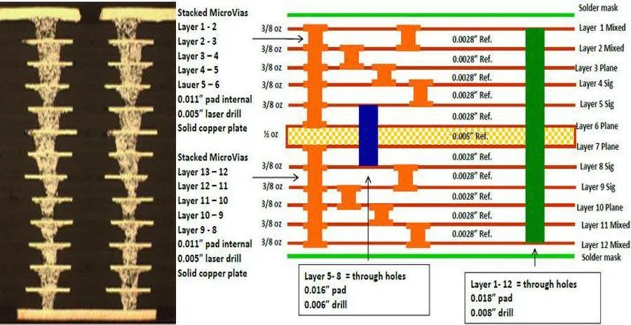
The process starts with a thin core, often 0.1 mm or less, followed by resin-coated copper (RCC) or prepreg lamination. Laser drilling targets specific layers, and conductive or non-conductive fills are applied to maintain planarity. Curing and plating steps follow, with registration accuracy held to plus or minus 50 microns. This controlled buildup minimizes drill breakout and ensures via-in-pad reliability during subsequent assembly. Factories optimize sequential lamination by selecting low-CTE materials to match component requirements.
Microvia Filling Techniques for Reliable Via-in-Pad
Microvia filling is the cornerstone of via-in-pad technology, using conductive pastes, electroplated copper, or non-conductive epoxies to plug laser-drilled holes. Conductive fills provide electrical continuity through the via while allowing pad plating, ideal for stacked configurations in sequential lamination. Non-conductive fills prioritize planarity and thermal stability, preventing solder wicking during reflow. Filling must achieve 100 percent void-free coverage to pass reliability tests like thermal shock and intermetallic growth assessments. IPC-2226 guidelines outline design rules for fill selection based on via diameter and depth.
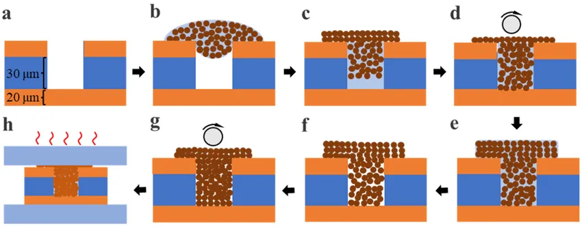
In practice, screen-printed conductive paste offers cost-effective filling for vias up to 100 microns in diameter, followed by electroplating to build copper walls. For deeper stacked vias, multiple fill-plating cycles during sequential lamination ensure uniformity. Post-fill planarization via grinding or chemical etching creates a smooth surface for fine-pitch soldering. Engineers should verify fill conductivity with four-point probe testing before lamination. These techniques directly enhance HDI PCB component density by enabling pad reuse.
Three primary approaches exist:
| Material Type | Void Rate Target | Thermal Conductivity | Relative Cost | Reflow Compatibility (260°C) | Best Use Cases |
|---|---|---|---|---|---|
| Conductive Paste | <2% | Moderate | Low | Good | Cost-sensitive consumer electronics, non-critical signals |
| Non-Conductive Epoxy | <1% | Low | Medium | Excellent | Standard via-in-pad, planarity-critical BGAs |
| Electroplated Copper | <0.5% | High | Higher | Superior | High-reliability (automotive, 5G, aerospace), stacked vias, thermal pads |
Design and Manufacturing Best Practices
Designing for sequential lamination and via-in-pad starts with stackup planning to balance microvia staggering and core thickness. Pad sizes must exceed via diameter by at least 75 microns on all sides to accommodate drill tolerances and plating buildup. Simulate thermal profiles early to predict fill material behavior under reflow peaks of 260 degrees Celsius. Manufacturing teams employ automated optical inspection (AOI) after each lamination step to detect fill voids or misalignment. Engineers should also consult our microvia filling techniques and reliability guide when specifying fill materials.
Best practices include using photosensitive soldermasks over via-in-pad to prevent solder exposure during advanced PCB assembly. Sequential lamination schedules should incorporate intermediate b-stage cures to control flow during pressing. For high-volume production, validate processes against J-STD-001 for soldering acceptability. Troubleshooting common issues like via cratering involves adjusting laser parameters and fill viscosity. These steps ensure maximum component density without yield losses.
Challenges and Solutions in High-Density Implementation
Warpage remains a key challenge in sequential lamination due to asymmetric buildup and CTE mismatches between cores and build-ups. Solutions involve symmetric stackups where possible or carrier panels for thin cores during processing. Via-in-pad reliability under vibration calls for reinforced fills with high glass transition temperatures. Electrical testing, including flying probe for opens and shorts, confirms integrity post-lamination.
In advanced PCB assembly, via-in-pad demands precise stencil design to avoid paste starvation around filled areas. Nitrogen reflow atmospheres minimize oxidation on plated surfaces. Factories monitor these via X-ray inspection for fill density. Addressing these hurdles unlocks the full potential of HDI PCB component density.
Advanced Testing, Reliability, and Validation Strategies
Beyond basic AOI and flying probe, high-reliability via-in-pad HDI boards require:
- X-ray and 3D CT for void detection (<50 µm voids rejected).
- Microsection analysis on test coupons to verify plating thickness, fill quality, and intermetallic layers.
- Thermal cycling and shock per IPC-6012DS (typically −55°C to +125°C or harsher for automotive).
- ** IST (Interconnect Stress Testing)** or IST coupons to predict via life.
- Vibration and mechanical shock for aerospace/automotive qualification.
- C-scan acoustic microscopy for delamination detection post-reflow.
Digital traceability and statistical process control close the loop on continuous improvement. In 2026, AI-powered optical inspection systems flag anomalies in real time with >99% accuracy.
Cost Analysis and ROI of Via-in-Pad Sequential Lamination
Sequential lamination increases fabrication cost due to multiple drill-fill-plate cycles (roughly 20–40% premium per additional cycle versus standard multilayer). However, the ability to reduce overall layer count, shrink board size by 20–35%, and improve yields often delivers strong ROI.
For a typical 5G module, via-in-pad + sequential lamination can cut board area by 25%, lowering material and assembly costs while improving signal performance. Break-even is usually reached at mid-volume (5,000–20,000 units). High-reliability markets (automotive, medical) see faster payback through reduced field failures. Always perform a detailed cost-benefit analysis with your fabricator, factoring in reduced layer count and improved routing efficiency.
Real-World Case Studies and Lessons Learned
Case Study 1: 5G mmWave Module (2025–2026 Deployment)
A leading infrastructure supplier transitioned a 28 GHz front-end from traditional fanout to via-in-pad with 2+N+2 sequential lamination using electroplated copper fill. Component density increased 35%, layer count dropped from 8 to 6, and insertion loss improved by 1.1 dB. Key lesson: tight impedance control (±5%) and early DFM reviews with the fabricator raised first-pass yield from 78% to 94%. X-ray validation of every panel was critical.
Case Study 2: Automotive 77 GHz Radar Sensor
An automotive Tier-1 adopted any-layer HDI with via-in-pad for a next-generation ADAS radar. Low-CTE build-up films and copper-filled vias enabled a 40% smaller module footprint while passing AEC-Q100 Grade 2 reliability. Warpage was controlled below 0.6% through symmetric stacking and carrier panels. Lesson learned: thermal simulation of the exact reflow profile prevented early delamination; AI-assisted AOI reduced inspection time by 60%. The project highlighted the value of close design–fab–assembly collaboration from concept stage.
Future Trends in HDI PCBs for 2026 and Beyond
In 2026 and beyond, expect wider adoption of modified semi-additive processes (mSAP) for lines/spaces below 30 µm, new low-CTE build-up films that survive 5+ sequential cycles without degradation, and embedded active/passive components. AI/ML inspection systems will become standard for real-time defect prediction during lamination and filling. Sustainability pressures are driving recyclable resins and lower environmental-impact plating chemistries while maintaining reliability.
Integration of photonics, higher power densities (>300 W/in² for AI accelerators), and ultra-HDI for 6G will push via-in-pad and sequential lamination even further. Designers who master these evolving tools will lead in compact, high-performance electronics.
Conclusion
Sequential lamination and via-in-pad technology represent pivotal advancements for engineers tackling space constraints in HDI PCBs. By enabling filled microvias within component pads, these processes dramatically increase routing and placement density while preserving signal quality. Microvia filling techniques and best practices ensure manufacturability and long-term reliability. As electronics evolve toward finer pitches, mastering sequential lamination for via-in-pad will define successful designs. Facilities adhering to standards like IPC-6012DS position themselves for cutting-edge production.
FAQs
Q1: What is the primary benefit of via-in-pad technology in HDI PCB component density?
A1: Via-in-pad allows microvias to occupy component pad space directly, eliminating fanout requirements and freeing surface area for more parts. This supports pitches under 0.4 mm, ideal for BGAs and CSPs. Sequential lamination ensures reliable stacking without planarity issues. Manufacturing focuses on void-free fills to maintain solder joint integrity during assembly.
Q2: How does sequential lamination for via-in-pad differ from standard buildup processes?
A2: Sequential lamination adds layers incrementally, permitting precise via drilling and filling between cycles, unlike all-at-once lamination that risks misalignment. This method supports stacked and staggered vias critical for via-in-pad. It controls warpage through intermediate cures and enhances HDI PCB component density. Factories achieve tighter tolerances with this approach.
Q3: Why is microvia filling essential for advanced PCB assembly with via-in-pad?
A3: Microvia filling creates a planar surface for soldering, preventing defects like wicking or voids in fine-pitch joints. Conductive fills maintain electrical paths through pads, supporting high-density routing. It withstands reflow stresses per industry standards. This step maximizes component placement without compromising assembly yields.
Q4: What design rules apply to via-in-pad in sequential lamination HDI PCBs?
A4: Keep via-to-pad annular ring at minimum 75 microns and aspect ratios at 1:1 for reliable plating. Plan stackups for microvia staggering to avoid breakout. Verify fill planarity post-lamination for SMT compatibility. These rules boost HDI PCB component density while ensuring manufacturability.
References
IPC-6012DS — Qualification and Performance Specification for High Density Interconnect (HDI) Printed Boards. IPC, 2017
IPC-2226 — Design Standard for Printed Electronics on Rigid Printed Board Substrates. IPC, 2018
J-STD-001H — Requirements for Soldered Electrical and Electronic Assemblies. IPC, 2020