Introduction
High-frequency PCB assembly is a critical process in modern electronics, especially for applications in telecommunications, aerospace, and advanced computing. These boards operate at frequencies above 100 MHz, requiring precise assembly techniques to ensure signal integrity and minimal interference. This guide provides a detailed walkthrough of the assembly process, focusing on surface mount technology (SMT), through-hole components, reflow soldering, and automated optical inspection (AOI). Whether you are an electrical engineer or a technical professional, understanding these steps is essential for achieving reliable performance in high-frequency designs. The following sections break down the complexities of PCB assembly, offering practical insights and best practices aligned with industry standards to help you navigate the challenges of working with high-frequency circuits.
What Is High-Frequency PCB Assembly and Why It Matters
High-frequency PCB assembly involves the precise placement and soldering of components on printed circuit boards designed to handle rapid signal transitions. These boards are integral to devices like RF transceivers, radar systems, and 5G infrastructure, where signal loss or noise can compromise functionality. The assembly process must account for unique challenges such as impedance control, thermal management, and electromagnetic interference. Proper execution ensures the board performs as intended under demanding conditions. Unlike standard PCB assembly, high-frequency applications require tighter tolerances and specialized materials, making attention to detail during SMT, through-hole integration, reflow soldering, and AOI inspection vital for success. Neglecting these factors can lead to costly failures in critical systems.
Technical Principles of High-Frequency PCB Assembly
High-frequency PCB assembly demands a deep understanding of electrical and thermal dynamics. At elevated frequencies, signals are prone to loss due to skin effect, where current flows near the conductor’s surface, increasing resistance. Dielectric materials must also be chosen carefully to minimize signal attenuation. Assembly techniques like SMT and through-hole mounting must ensure precise alignment to avoid parasitic capacitance or inductance. Reflow soldering, a common method for SMT, requires controlled temperature profiles to prevent component damage or solder joint defects. Additionally, AOI systems play a crucial role in detecting misalignments or soldering flaws that could disrupt high-frequency performance. Each step in the process directly impacts the board’s ability to maintain signal integrity.
Key Considerations for High-Frequency Designs
Several factors influence the success of high-frequency PCB assembly:
- Material Selection: Low-loss dielectrics and high-conductivity copper are essential.
- Component Placement: Close proximity of components can introduce crosstalk if not planned.
- Soldering Precision: Uniform solder joints prevent impedance mismatches.
- Inspection Rigor: AOI must be calibrated for fine-pitch components common in these designs.
Step-by-Step Guide to High-Frequency PCB Assembly
This section outlines the practical steps for assembling the high-frequency PCB, incorporating SMT, through-hole components, reflow soldering, and AOI best practices. Each phase is tailored to address the unique demands of high-frequency applications.
Step 1: Design Verification and Preparation
Before assembly begins, verify the PCB design for high-frequency compatibility. Ensure trace widths and spacing meet impedance requirements as per industry guidelines like IPC-2141. Confirm that the bill of materials specifies components rated for the intended frequency range. Prepare the assembly area to maintain cleanliness, as contaminants can affect solderability and signal performance. Static control measures are also critical to protect sensitive components during handling.
Step 2: Solder Paste Application for SMT
For SMT components, apply solder paste using a stencil aligned with the PCB’s surface pads. Precision is key in high-frequency assembly, as uneven paste can lead to poor solder joints. Use a stencil thickness that matches the component pitch, adhering to recommendations in IPC-7525 for stencil design. Inspect the paste deposit visually or with automated systems to ensure consistency before proceeding to component placement.
Step 3: SMT Component Placement
Place SMT components using automated pick-and-place machines for accuracy. High-frequency designs often include small, fine-pitch parts, so machine calibration must be exact. Position components to minimize signal path lengths and avoid interference between adjacent elements. Follow placement guidelines from IPC-A-610 for acceptable alignment tolerances. Double-check critical components like RF connectors or capacitors to ensure orientation matches the design schematic.
Step 4: Reflow Soldering for SMT
Reflow soldering attaches SMT components to the PCB through a controlled heating process. Use a temperature profile compliant with JEDEC J-STD-020E to prevent thermal shock to sensitive parts. For high-frequency PCBs, monitor the ramp-up and cooling rates closely to avoid warpage or solder defects. Preheat the board gradually, then reach peak temperatures only long enough to form reliable joints. Post-reflow, allow the board to cool naturally to minimize stress.
Step 5: Through-Hole Component Integration
Through-hole components are often used in high-frequency designs for power connectors or large inductors. Insert these manually or with automated equipment, ensuring leads align with PCB holes. Solder using wave soldering or selective soldering methods, following IPC-A-610 standards for joint quality. Pay attention to lead length and pad clearance to avoid interference with nearby high-frequency traces. Inspect each joint for proper fillet formation after soldering.
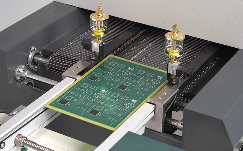
Step 6: Automated Optical Inspection (AOI)
AOI is indispensable for verifying assembly quality in high-frequency PCBs. Use AOI systems to check for misaligned components, solder bridges, or insufficient joints. Calibrate the system to detect defects in fine-pitch SMT parts, adhering to IPC-A-600K for acceptability criteria. Focus on critical areas like RF sections where even minor flaws can degrade performance. Document any issues for rework before moving to functional testing.
Step 7: Cleaning and Final Inspection
After soldering and AOI, clean the PCB to remove flux residues that could affect high-frequency signals. Use approved cleaning agents and methods as per IPC-CH-65 for post-solder cleaning. Conduct a final visual inspection to confirm no debris or damage remains. Test the board under simulated operating conditions to validate signal integrity and performance against design specifications.
Best Practices for High-Frequency PCB Assembly
Achieving optimal results in high-frequency PCBA assembly requires adherence to proven practices. Always use fixtures or supports during reflow soldering to prevent board warpage, a common issue with thin, high-frequency substrates. Maintain strict environmental controls, including humidity and temperature, to protect components and materials. Train personnel on handling procedures to avoid static discharge or physical damage. Regularly calibrate assembly and inspection equipment to ensure precision. Finally, document every step of the process for traceability, aligning with quality management principles in ISO 9001:2015.
Troubleshooting Common Issues in High-Frequency PCB Assembly
High-frequency PCB assembly can encounter specific challenges. Signal degradation often results from poor solder joints or misaligned components, detectable through AOI and reworkable per IPC-7711/7721 guidelines. Tombstoning in SMT parts may occur due to uneven heating during reflow soldering; adjust the temperature profile to balance thermal distribution. Through-hole components might exhibit insufficient solder fill, requiring inspection against IPC-A-610 criteria and manual touch-up if needed. Address these issues promptly to prevent cascading failures in the final product.
Conclusion
High-frequency PCB assembly is a meticulous process that demands precision at every stage, from SMT placement and reflow soldering to through-hole integration and AOI verification. By following the outlined steps and adhering to industry standards, engineers can ensure reliable performance in demanding applications. Attention to material selection, equipment calibration, and environmental control is non-negotiable for maintaining signal integrity. This guide serves as a practical resource for navigating the complexities of high-frequency designs, empowering professionals to achieve consistent, high-quality results in their projects.
FAQs
Q1: What are the key challenges in high-frequency PCB assembly?
A1: High-frequency PCB assembly faces issues like signal loss, electromagnetic interference, and impedance mismatches. Precise SMT placement and reflow soldering are crucial to avoid parasitic effects. Materials must minimize dielectric loss, and AOI helps detect subtle defects. Following strict standards ensures reliability in applications like RF systems.
Q2: How does reflow soldering impact high-frequency PCB performance?
A2: Reflow soldering must be carefully controlled in high-frequency PCB assembly to prevent thermal stress or warpage. Uneven heating can cause poor solder joints, affecting signal integrity. Adhering to profiles in JEDEC J-STD-020E ensures components are not damaged, maintaining performance in critical circuits.
Q3: Why is AOI critical for high-frequency PCB assembly?
A3: AOI is vital in high-frequency PCB assembly for detecting misalignments or soldering flaws that disrupt signal paths. Fine-pitch SMT components require rigorous inspection per IPC-A-600K standards. Early defect identification prevents failures in high-stakes applications, ensuring the board meets design expectations.
Q4: How do through-hole components fit into high-frequency PCB assembly?
A4: Through-hole components are used for robust connections in high-frequency PCB assembly, often for power or grounding. Their integration requires precise soldering to avoid interference with nearby traces. Standards like IPC-A-610 guide joint quality, ensuring reliability without compromising the board’s high-frequency performance.
References
IPC-A-610H — Acceptability of Electronic Assemblies. IPC, 2020.
IPC-A-600K — Acceptability of Printed Boards. IPC, 2020.
JEDEC J-STD-020E — Moisture/Reflow Sensitivity Classification for Nonhermetic Surface Mount Devices. JEDEC, 2014.
IPC-7525B — Stencil Design Guidelines. IPC, 2011.
IPC-2141A — Design Guide for High-Speed Controlled Impedance Circuit Boards. IPC, 2004.
IPC-CH-65B — Guidelines for Cleaning of Printed Boards and Assemblies. IPC, 2011.
IPC-7711/7721C — Rework, Modification and Repair of Electronic Assemblies. IPC, 2017.
ISO 9001:2015 — Quality Management Systems. ISO, 2015.


