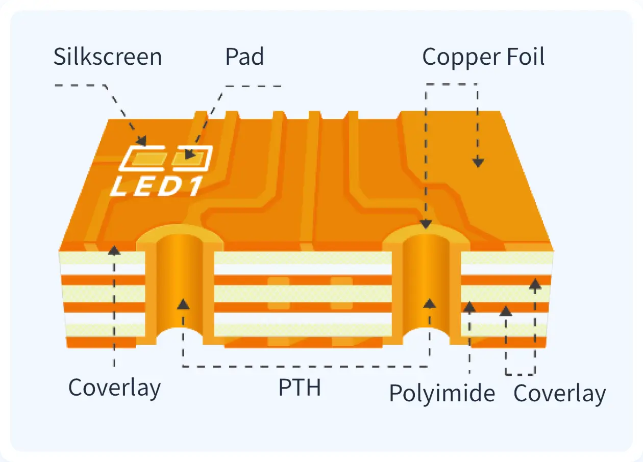
Introduction
Polyimide PCBs stand out in demanding applications such as aerospace, automotive electronics, and high-temperature sensors due to their exceptional thermal stability and flexibility. These boards, often used in rigid-flex configurations, require precise via formation to achieve high-density interconnects without compromising reliability. However, the unique properties of polyimide substrates, including high toughness and low thermal conductivity, introduce significant drilling challenges polyimide engineers must address. Advanced drilling techniques, particularly laser drilling polyimide methods, have become essential for meeting the precision demands of modern electronics. This article explores mechanical and laser approaches to polyimide PCB drilling, highlighting best practices for quality assurance. By understanding these techniques, electrical engineers can optimize designs for manufacturability and performance.
Why Polyimide PCBs Demand Specialized Drilling Techniques
Polyimide materials excel in environments exceeding 200 degrees Celsius continuously, making them ideal for applications where standard FR-4 substrates fail. Yet, this durability translates to polyimide PCB drilling difficulties, as the polymer resists conventional cutting tools effectively. Engineers face issues like excessive tool wear, heat-induced delamination, and inconsistent hole geometries that can lead to plating failures downstream. Specialized techniques ensure vias meet aspect ratios up to 1:1 reliably, supporting multilayer stacks in compact designs. The shift toward higher interconnect densities in HDI boards further amplifies the need for microvia capabilities beyond mechanical limits. Ultimately, selecting the right drilling method aligns production with performance goals in harsh operating conditions.
Key Drilling Challenges in Polyimide PCBs
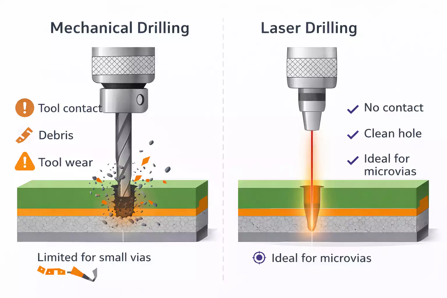
Drilling challenges polyimide substrates present stem primarily from their mechanical hardness and sensitivity to thermal stress. Mechanical processes generate friction heat that softens the resin, causing smear on hole walls and potential cracking in adjacent layers. The abrasive nature accelerates drill bit dulling, increasing breakout roughness and risking fiberglass protrusion if reinforced variants are used. In flexible polyimide films, warpage during drilling exacerbates positional accuracy, complicating registration for subsequent plating. Laser alternatives mitigate these by ablating material without contact, but they introduce concerns like heat-affected zones if parameters are not tuned precisely. Addressing these requires process controls aligned with industry benchmarks for hole quality and reliability.
Mechanical Drilling for Polyimide PCBs
Mechanical drilling polyimide remains viable for through-holes larger than 150 microns in thicker rigid sections of polyimide PCBs. High-spindle speeds exceeding 100,000 RPM combined with peck cycles minimize heat buildup by allowing chip evacuation between advances. Entry and backup materials protect surface finish, reducing burr formation critical for plating adhesion. Feed rates must balance penetration efficiency against tool life, often necessitating diamond-coated bits for abrasion resistance. While cost-effective for production volumes, limitations in microvia formation push designs toward hybrid approaches in high-density boards. Quality verification involves measuring hole wall roughness and taper per IPC-6012E specifications to ensure plating integrity.
Engineers optimize mechanical drilling polyimide by adjusting parameters based on stack height and copper thickness. Thinner stacks tolerate higher feeds, while multilayers demand conservative settings to prevent exit-side defects. Post-drill desmear using plasma or chemical permanganate removes resin residue, preparing surfaces for electroless copper deposition. Inspection via automated optical systems detects oversize or out-of-round holes early. Despite advancements, mechanical methods struggle with blind vias in polyimide, where laser takes precedence. Consistent application yields reliable interconnects when via diameters suit the technique.
Laser Drilling Techniques for Polyimide Substrates
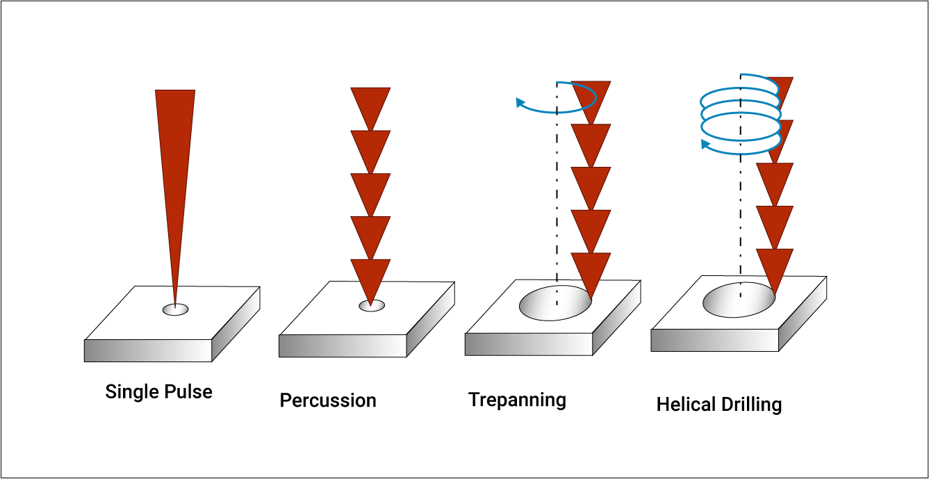
Laser drilling polyimide has revolutionized polyimide PCB via formation, enabling vias as small as 50 microns with superior edge quality. UV lasers, such as excimer at 308 nm or 355 nm harmonics, excel due to polyimide's strong absorption, minimizing thermal damage through photochemical ablation. CO2 lasers at 10.6 microns work via thermal vaporization but require pulse shaping to control taper in deeper holes. Femtosecond ultrafast lasers further reduce heat-affected zones, ideal for stacked microvias in rigid-flex polyimides. Process parameters like fluence, repetition rate, and assist gas influence hole profile and debris removal. These non-contact methods preserve substrate integrity, crucial for flexible circuits prone to mechanical stress.
In practice, direct ablation suits blind vias, while mask projection accelerates throughput for arrays. Polyimide's low ablation threshold allows clean sidewalls without recast layers common in metals. Overlapping pulses ensure flat bottoms, vital for filled via applications. Post-laser cleaning via plasma desmear or wet processing eliminates carbon residue from ablation. Alignment systems with fiducials achieve sub-micron accuracy, supporting HDI densities. Laser drilling polyimide thus bridges design aspirations with fabrication feasibility in advanced packages.
Advanced Polyimide PCB Via Formation Strategies
Polyimide PCB via formation integrates mechanical and laser drilling in hybrid flows for optimal layer transitions. Stacked vias, drilled sequentially post-lamination, demand precise depth control to avoid stubs, while staggered configurations reduce aspect ratios. Laser facilitates any-layer vias in HDI polyimide boards, enabling fanout from fine-pitch components. Sequential build-up processes layer dielectrics with laser vias, followed by copper filling via electroplating for planar surfaces. Challenges like via chaining in flex regions require reinforced adhesives to maintain alignment. Factory insights emphasize pilot runs to calibrate for material variations, ensuring yield.
Best practices include simulation of thermal profiles during drilling to predict warpage. Cross-section analysis verifies annulus and capture pad integrity per IPC-A-600 criteria. Plasma treatment enhances desmear uniformity, critical for polyimide's inert surface. For high-reliability apps, bake-out precedes drilling to remove moisture, preventing voids. Integrating these steps aligns polyimide PCB drilling with qualification under IPC-6013 standards for flex circuits. Resulting boards exhibit robust thermal cycling performance.
Ensuring Precision and Quality in Production
Precision in polyimide PCB drilling hinges on metrology throughout the process. Automated drills feature closed-loop feedback for spindle runout below 5 microns, while laser galvos maintain beam spot consistency. In-line AOI coupled with laser triangulation measures hole diameter and depth post-drill. Electrical testing via flying probe confirms continuity before plating. Quality gates reject lots exceeding roughness limits, safeguarding downstream assembly. Documented process controls, including SPC on hit rates, support traceability.
Troubleshooting common defects involves root cause analysis: excessive taper signals improper pulse energy, while rough walls indicate inadequate desmear. Adjusting chipload in mechanical or fluence in laser resolves most issues. Collaboration between design and fab teams refines drill files for optimal entry angles. These measures ensure polyimide boards meet end-user reliability in vibration and thermal shock.
Conclusion
Advanced drilling techniques transform polyimide PCB challenges into opportunities for high-performance interconnects. Mechanical methods suit larger vias with cost efficiency, while laser drilling polyimide dominates microvia precision and flex compatibility. By tackling material-specific hurdles through tuned parameters and rigorous inspection, engineers achieve superior quality. Adhering to standards like IPC-6012E and IPC-A-600 guarantees qualification for demanding sectors. Hybrid strategies and process optimization will drive future densities. Electrical engineers benefit from specifying drill-friendly designs early for seamless production.
FAQs
Q1: What are the main drilling challenges polyimide PCBs face?
A1: Polyimide's high toughness causes rapid tool wear and heat buildup in mechanical drilling, leading to delamination and burrs. Laser drilling polyimide avoids contact stress but requires precise energy control to minimize heat-affected zones. Best practices include peck cycles for mechanical and optimized pulses for laser, with desmear ensuring plating readiness. Standards like IPC-A-600 guide acceptability for hole quality.
Q2: How does laser drilling polyimide compare to mechanical drilling polyimide?
A2: Laser excels in microvias under 100 microns with clean ablation, ideal for HDI polyimide PCB via formation, while mechanical suits larger through-holes cost-effectively. Mechanical risks smear and taper in tough polyimide, whereas laser preserves flexibility without mechanical deformation. Choose laser for density, mechanical for thickness. Hybrid use optimizes both.
Q3: What best practices improve polyimide PCB drilling outcomes?
A3: Select UV lasers for photochemical ablation in polyimide to reduce thermal damage, and use high-RPM spindles with diamond bits for mechanical. Implement plasma desmear and AOI inspection post-drill for precision. Control stackup warpage with fixtures. These align with IPC-6013 for flex reliability.
Q4: Why is precision critical in polyimide PCB via formation?
A4: Precise vias ensure reliable plating and signal integrity in high-temp polyimide applications. Poor drilling causes opens or shorts, failing thermal cycling. Laser techniques achieve sub-micron accuracy, supporting fine-pitch BGA. Quality controls per industry standards prevent field failures.
References
IPC-6012E — Qualification and Performance Specification for Rigid Printed Boards. IPC, 2017
IPC-A-600K — Acceptability of Printed Boards. IPC, 2020
IPC-6013D — Qualification and Performance Specification for Flexible and Rigid-Flex Printed Boards. IPC, 2014


