Introduction
High Density Interconnect (HDI) PCBs are at the forefront of modern electronics, enabling compact designs with superior functionality. These boards are essential for applications requiring high speed and reliability, such as telecommunications, medical devices, and aerospace systems. A critical aspect of HDI PCB design is the selection of stackup materials, which directly impacts signal performance. Materials with specific properties, such as low Dk, low loss, and high Tg, are vital for maintaining signal integrity and impedance control. For electrical engineers, understanding HDI PCB stackup materials is key to optimizing performance in demanding environments. This article explores the role of low Dk materials, low loss materials, high Tg materials, and impedance control materials in achieving exceptional signal quality.
What Is HDI PCB Stackup and Why It Matters
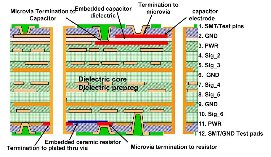
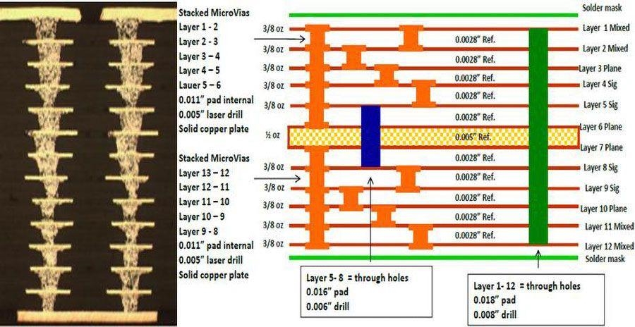
HDI PCB stackup refers to the arrangement of conductive and insulating layers in a printed circuit board designed for high density. Unlike traditional PCBs, HDI boards feature finer traces, smaller vias, and denser component placement. This configuration supports miniaturization while accommodating complex circuitry. The choice of materials in the stackup determines electrical performance, thermal stability, and mechanical strength.
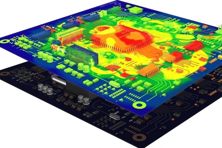
Signal performance is a primary concern in high speed applications. Poor material selection can lead to signal loss, crosstalk, and impedance mismatches. For engineers working on cutting edge designs, selecting appropriate HDI PCB stackup materials ensures data integrity and reduces electromagnetic interference. As devices operate at higher frequencies, the need for low Dk materials and low loss materials becomes even more pronounced. Proper stackup design also aids in impedance control, a crucial factor for consistent signal transmission.
Technical Principles of HDI PCB Stackup Materials
Dielectric Constant and Low Dk Materials
The dielectric constant, or Dk, measures a material's ability to store electrical energy in an electric field. Low Dk materials are preferred in HDI PCB stackups for high speed applications. A lower Dk value reduces signal propagation delay, enabling faster data transfer. This property is essential for maintaining signal integrity in circuits operating at gigahertz frequencies.
Materials with low Dk values minimize capacitance between adjacent traces, reducing crosstalk. Engineers often prioritize these materials in multilayer HDI designs to support dense routing without performance degradation. Standards such as IPC-4101E provide guidelines for selecting base materials with specific dielectric properties for high performance boards.
Dissipation Factor and Low Loss Materials
The dissipation factor, or Df, indicates the energy loss in a dielectric material under an alternating electric field. Low loss materials, characterized by a low Df, are critical for minimizing signal attenuation in HDI PCBs. At high frequencies, energy loss can distort signals, impacting system reliability.
Using low loss materials in stackup design ensures that signals maintain their strength over longer traces. This is particularly important in telecommunications and RF applications where signal clarity is paramount. Engineers must balance low loss properties with other material characteristics to meet design requirements. Testing per IPC-TM-650 standards helps validate the performance of these materials under real world conditions.
Thermal Stability and High Tg Materials
Glass transition temperature, or Tg, defines the point at which a material transitions from a rigid to a more flexible state. High Tg materials are essential for HDI PCB stackups in environments with elevated temperatures. These materials resist deformation during thermal cycling, ensuring structural integrity.
In applications like automotive electronics, where boards face significant heat, high Tg materials prevent delamination and warping. They also support consistent electrical performance under stress. Standards such as IPC-4101E specify minimum Tg values for materials used in high reliability designs, guiding engineers in material selection.
Impedance Control and Material Selection
Impedance control is a cornerstone of high speed PCB design. It ensures that signals travel without reflection or distortion. Achieving controlled impedance in HDI PCBs requires precise material selection and layer arrangement. The dielectric thickness and Dk value of stackup materials directly influence impedance.
Materials designed for impedance control maintain consistent electrical properties across the board. Engineers use simulation tools to predict impedance based on material data, adhering to guidelines in IPC-2226 for HDI design. Proper stackup configuration, paired with suitable impedance control materials, minimizes signal mismatches in critical applications.
Suggested Reading: Advanced HDI PCB Stackup Materials for Improved Signal Performance
Best Practices for Selecting HDI PCB Stackup Materials
Evaluate Application Requirements
Before choosing HDI PCB stackup materials, engineers must assess the specific needs of their project. High speed digital circuits may prioritize low Dk materials and low loss materials to reduce signal delay and attenuation. In contrast, applications in harsh environments might focus on high Tg materials for thermal resilience.
Consider Layer Configuration
The arrangement of layers in an HDI stackup affects both electrical and mechanical performance. Alternating signal and ground layers can enhance impedance control and reduce noise. Engineers should select materials that support uniform dielectric thickness to maintain consistent impedance across layers.
Adhere to Industry Standards
Compliance with recognized standards ensures material reliability. For instance, IPC-6012E outlines performance specifications for rigid printed boards, including HDI designs. Following such standards helps in selecting materials that meet electrical and thermal benchmarks for specific applications.
Test for Signal Integrity
Simulating and testing signal integrity during the design phase is crucial. Engineers should use materials with known properties, validated through methods in IPC-TM-650, to predict performance. This approach identifies potential issues with signal loss or crosstalk before manufacturing.
Balance Cost and Performance
While advanced materials like low loss and high Tg options offer superior performance, they often come at a higher cost. Engineers must weigh these benefits against budget constraints. Selecting materials that meet essential requirements without over specification can optimize both cost and functionality.
Insight for Electrical Engineers
For electrical engineers, the challenge lies in integrating multiple material properties into a cohesive HDI PCB stackup design. A common issue is balancing low Dk materials with thermal demands. While low Dk options enhance signal speed, they may not always offer the necessary thermal stability for high power applications. In such cases, a hybrid approach using different materials for specific layers can be effective.
Another consideration is the impact of manufacturing processes on material performance. Thermal stress during lamination can alter dielectric properties, affecting impedance control. Engineers should collaborate with fabrication teams to ensure that chosen materials maintain their characteristics post processing. Referencing standards like IPC-A-600K for acceptability criteria aids in maintaining quality throughout production.
Conclusion
Selecting the right HDI PCB stackup materials is fundamental to achieving improved signal performance in modern electronics. Low Dk materials reduce signal delays, while low loss materials minimize attenuation at high frequencies. High Tg materials ensure thermal stability, and impedance control materials maintain consistent signal paths. By understanding these properties and adhering to industry standards, electrical engineers can design HDI PCBs that meet the demands of cutting edge applications. A strategic approach to material selection, combined with rigorous testing, paves the way for reliable and efficient circuit designs.
FAQs
Q1: What are the benefits of using low Dk materials in HDI PCB stackup designs?
A1: Low Dk materials lower the dielectric constant, reducing signal propagation delay in HDI PCB stackup designs. This property is vital for high speed applications, as it minimizes capacitance between traces and decreases crosstalk. By incorporating these materials, engineers can achieve faster data transfer and maintain signal integrity, especially in dense multilayer configurations where performance is critical.
Q2: How do low loss materials impact signal performance in HDI PCBs?
A2: Low loss materials, with a low dissipation factor, reduce energy loss in HDI PCBs during signal transmission. They help maintain signal strength over long traces, which is essential for high frequency applications. Using these materials ensures minimal attenuation, improving overall system reliability and clarity in demanding environments like telecommunications and RF circuits.
Q3: Why are high Tg materials important for HDI PCB stackups?
A3: High Tg materials provide thermal stability in HDI PCB stackups by resisting deformation at elevated temperatures. They prevent issues like delamination and warping during thermal cycling, which is crucial for applications in harsh conditions such as automotive electronics. These materials ensure structural integrity and consistent electrical performance under thermal stress.
Q4: How do impedance control materials contribute to HDI PCB performance?
A4: Impedance control materials maintain consistent electrical properties in HDI PCBs, ensuring signals travel without reflection or distortion. They support precise dielectric thickness and Dk values, critical for matching impedance in high speed designs. Using these materials helps engineers achieve reliable signal transmission, reducing mismatches and enhancing overall circuit performance.
References
IPC-4101E - Specification for Base Materials for Rigid and Multilayer Printed Boards. IPC, 2021.
IPC-6012E - Qualification and Performance Specification for Rigid Printed Boards. IPC, 2020.
IPC-2226 - Sectional Design Standard for High Density Interconnect (HDI) Printed Boards. IPC, 2003.
IPC-A-600K - Acceptability of Printed Boards. IPC, 2020.
IPC-TM-650 - Test Methods Manual. IPC, Various Dates.


