Introduction
In the realm of modern electronics, the demand for compact, high-performance devices drives innovation in printed circuit board (PCB) technology. Fine-line PCBs, characterized by narrow trace widths and tight spacing, are essential for high-density applications in industries like telecommunications, automotive, and consumer electronics. A critical component in their manufacturing is the solder mask, particularly liquid photoimageable (LPI) solder mask, which offers precision for fine features. This article explores advanced techniques in LPI solder mask application, focusing on achieving high resolution and supporting high-density PCBs. Aimed at electrical engineers, this discussion provides technical insights into optimizing solder mask processes for fine-line PCB designs, ensuring reliability and performance in demanding environments.
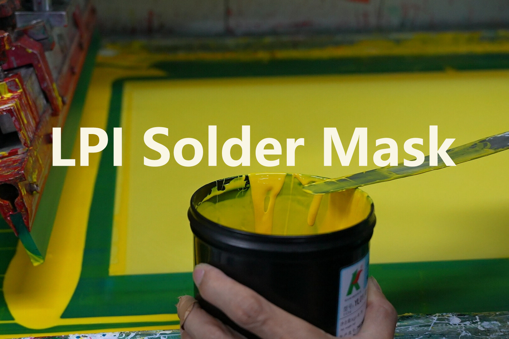
What Is Liquid Photoimageable Solder Mask and Why It Matters
Liquid photoimageable solder mask is a protective coating applied to PCBs to shield copper traces from oxidation and prevent solder bridging during assembly. Unlike traditional dry film masks, LPI solder mask is applied as a liquid and cured using ultraviolet light through a photolithographic process. This method allows for exceptional precision, making it ideal for fine-line PCB solder mask applications where trace widths can be as narrow as 50 micrometers or less. Its ability to form detailed patterns supports solder mask high resolution, crucial for high-density PCBs with closely spaced components.
The significance of LPI solder mask lies in its adaptability to complex designs. As electronic devices shrink, the need for high-density interconnects grows, pushing manufacturers to adopt technologies that accommodate solder mask fine features. Properly applied LPI solder mask ensures electrical insulation and enhances board durability, directly impacting the reliability of end products in critical applications.
Technical Principles of LPI Solder Mask for Fine-Line PCBs
The application of LPI solder mask involves several technical steps, each influencing the final quality of fine-line PCB solder mask. Understanding these principles helps engineers optimize processes for high resolution outcomes.
First, the liquid mask is coated onto the PCB surface using methods like curtain coating or screen printing. The coating thickness, typically between 10 to 30 micrometers, must be uniform to avoid defects in solder mask fine features. After coating, the board undergoes pre-baking to partially cure the mask, preparing it for exposure.
During exposure, ultraviolet light passes through a photomask to define the pattern. The precision of this step is vital for achieving solder mask high resolution, as any misalignment can result in incomplete coverage or overexposure. Advanced exposure systems with tight tolerances ensure accurate replication of fine patterns, especially for high-density PCBs.
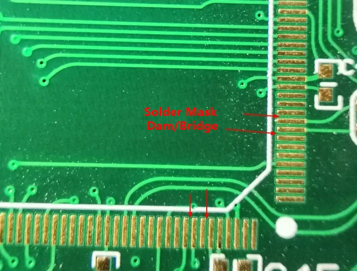
Post-exposure, the unexposed areas are removed using a developer solution, revealing the copper pads. The remaining mask is then fully cured through thermal baking, enhancing its mechanical and chemical resistance. For fine-line designs, controlling the development process is critical to prevent undercutting or residue that could compromise solder mask dam structures, which are narrow barriers between pads.
Challenges in Achieving Solder Mask Fine Features
Implementing LPI solder mask on fine-line PCBs presents unique challenges. One primary issue is maintaining resolution as feature sizes decrease. Narrow traces and small pad openings require precise alignment and exposure control to avoid defects like mask bleed or incomplete curing. Such defects can lead to short circuits or poor adhesion in high-density PCBs.
Another challenge is the formation of solder mask dam structures. These are essential for preventing solder bridging between closely spaced pads, especially in fine-pitch components. However, creating a stable dam with minimal width demands advanced materials and process control to ensure structural integrity without compromising adjacent features.
Environmental factors, such as humidity and temperature during processing, also affect outcomes. Variations can alter the viscosity of the liquid mask or the curing rate, impacting uniformity. Engineers must account for these variables to maintain consistent solder mask high resolution across production batches.
Practical Solutions for Optimizing LPI Solder Mask Techniques
Material Selection for High Resolution
Choosing the right LPI solder mask material is fundamental. Materials with high photosensitivity and low viscosity ensure better flow and coverage over intricate geometries. Additionally, selecting a mask with strong adhesion properties prevents delamination during thermal cycling or assembly processes, a common concern in high-density PCBs.
Process Parameter Control
Tight control over process parameters enhances solder mask fine features. Exposure energy must be calibrated to match the mask thickness and desired resolution. Overexposure can cause feature distortion, while underexposure may leave uncured areas. Similarly, development time and solution concentration should be optimized to avoid undercutting or residue on fine-line patterns.
Advanced Imaging Techniques
Utilizing high-precision imaging systems improves pattern accuracy. Laser direct imaging (LDI) is one such technique that eliminates the need for physical photomasks, reducing alignment errors. LDI enables finer resolution by directly transferring digital designs onto the mask layer, ideal for complex high-density PCBs requiring solder mask high resolution.
Solder Mask Dam Optimization
For effective solder mask dam structures, engineers can adjust the mask design to balance width and height. A dam that is too narrow risks collapsing, while one too wide may encroach on pad areas. Simulation tools can predict dam performance under various conditions, guiding design adjustments before production.
Environmental Monitoring
Maintaining a controlled environment during application and curing minimizes defects. Temperature and humidity levels should align with material specifications to ensure consistent curing and adhesion. Automated monitoring systems can track these variables, providing real-time feedback for process adjustments.
Industry Standards for Solder Mask Application
Adherence to recognized industry standards ensures the quality and reliability of LPI solder mask processes for fine-line PCBs. Standards provide guidelines on material properties, application methods, and performance criteria, helping engineers achieve consistent results.
The IPC-SM-840E standard, titled Qualification and Performance of Permanent Solder Mask and Flexible Cover Materials, outlines requirements for solder mask materials, including adhesion, thermal resistance, and chemical durability. Compliance with this standard ensures that the solder mask withstands assembly and operational stresses, particularly in high-density PCBs.
Additionally, IPC-6012E, known as Qualification and Performance Specification for Rigid Printed Boards, specifies acceptance criteria for solder mask coverage and registration. Following these guidelines helps maintain solder mask fine features and prevents defects like misalignment or incomplete coverage.
Troubleshooting Common Issues in Fine-Line Solder Mask Application
Even with optimized processes, issues can arise during LPI solder mask application. Identifying and addressing these problems promptly preserves board quality. One common issue is poor registration, where the mask does not align with copper features. This can result from equipment misalignment or photomask distortion. Regular calibration of exposure systems mitigates this risk.
Another frequent problem is incomplete curing, leading to soft or tacky mask areas. This often stems from insufficient exposure energy or inadequate thermal baking. Adjusting process parameters or verifying equipment settings resolves this issue. For high-density PCBs, ensuring uniform curing across the board surface is essential to avoid weak spots.
Bubble formation or voids in the mask layer can also occur due to trapped air or contaminants during coating. Implementing vacuum-assisted coating techniques or enhancing surface cleaning protocols before application reduces such defects, ensuring robust solder mask dam structures.
Conclusion
Advanced liquid photoimageable solder mask techniques are pivotal for the successful fabrication of fine-line PCBs, enabling high-density designs with precise solder mask high resolution. By understanding the technical principles, addressing challenges, and implementing best practices, engineers can optimize the application process for solder mask fine features. Adherence to industry standards like IPC-SM-840E and IPC-6012E ensures consistent quality and reliability. As electronics continue to evolve toward miniaturization, mastering these techniques remains essential for meeting the demands of cutting-edge applications.
FAQs
Q1: How does liquid photoimageable solder mask improve fine-line PCB performance?
A1: Liquid photoimageable solder mask enhances fine-line PCB performance by providing precise coverage over narrow traces and tight spaces. Its photolithographic process ensures high resolution, preventing solder bridging and protecting copper from oxidation. This precision is vital for maintaining electrical integrity in compact designs, supporting reliable operation in demanding applications.
Q2: What are the key factors for achieving solder mask high resolution in high-density PCBs?
A2: Achieving solder mask high resolution in high-density PCBs requires precise control over exposure energy, development time, and material selection. High-photosensitivity masks and advanced imaging techniques like laser direct imaging improve pattern accuracy. Consistent environmental conditions and equipment calibration also play critical roles in ensuring detailed and defect-free results.
Q3: Why is a solder mask dam important for fine-pitch components?
A3: A solder mask dam is crucial for fine-pitch components as it acts as a barrier between closely spaced pads, preventing solder bridging during assembly. This structure ensures proper solder joint formation, reducing the risk of short circuits. Its design must balance width and stability to maintain effectiveness without interfering with pad areas.
Q4: How do industry standards guide solder mask application for fine-line PCB solder mask?
A4: Industry standards like IPC-SM-840E and IPC-6012E provide guidelines for solder mask material performance and application quality. They specify requirements for adhesion, coverage, and thermal resistance, ensuring the fine-line PCB solder mask withstands assembly and operational stresses. Compliance with these standards guarantees consistent reliability across production batches.
References
IPC-SM-840E — Qualification and Performance of Permanent Solder Mask and Flexible Cover Materials. IPC, 2010.
IPC-6012E — Qualification and Performance Specification for Rigid Printed Boards. IPC, 2020.


