Introduction
Radio Frequency (RF) PCB design stands as a critical discipline in modern electronics, especially for applications in telecommunications, aerospace, and IoT devices. Unlike standard PCB layouts, RF designs operate at high frequencies, where signal integrity, impedance control, and electromagnetic interference become paramount concerns. Mastering RF PCB routing techniques, such as microstrip design, stripline design, and coplanar waveguide structures, is essential for electrical engineers aiming to achieve optimal performance. This article explores advanced strategies for RF PCB transmission line design, focusing on trace impedance control and layout considerations. By understanding the nuances of these techniques, engineers can minimize signal loss and ensure reliable operation in high frequency environments. Let's delve into the principles and practical approaches that define successful RF PCB implementations.
What Are RF PCB Routing Techniques and Why Do They Matter
RF PCB routing techniques involve specialized methods to design and lay out transmission lines that carry high frequency signals. These signals, often in the range of hundreds of megahertz to several gigahertz, are highly sensitive to layout variations. Poor routing can lead to signal degradation, crosstalk, or unwanted emissions, impacting device performance. Techniques like microstrip design, where a conductor is placed on the surface of a dielectric above a ground plane, and stripline design, where the conductor is embedded between two ground planes, are fundamental to maintaining signal integrity. RF PCB coplanar waveguide structures offer another approach by placing ground planes adjacent to the signal trace on the same layer. These methods matter because they directly influence impedance matching and noise reduction, ensuring efficient power transfer and compliance with stringent industry standards.
Technical Principles of RF PCB Routing
Microstrip Design Fundamentals
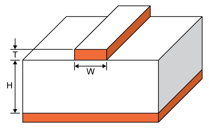
Microstrip design in RF PCBs consists of a conductive trace on the top layer of a dielectric substrate, with a ground plane beneath. This configuration is widely used due to its simplicity and ease of fabrication. The impedance of a microstrip line depends on the trace width, dielectric thickness, and the dielectric constant of the substrate material. At high frequencies, maintaining a consistent characteristic impedance, typically 50 ohms for many RF applications, is crucial to avoid reflections. Engineers must also account for parasitic effects like fringing fields, which can alter impedance if not properly managed. Careful selection of substrate materials with low loss tangent values helps minimize signal attenuation.
Stripline Design Characteristics
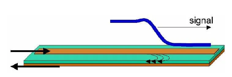
Stripline design places the signal trace between two parallel ground planes, fully embedded within the dielectric. This structure offers better shielding compared to microstrip, reducing electromagnetic interference and crosstalk. The symmetry of the ground planes ensures a more uniform electric field distribution, which aids in achieving precise impedance control. However, stripline designs are more complex to fabricate due to the multilayer construction, and accessing the trace for testing or modifications can be challenging. The dielectric constant and the spacing between ground planes play a significant role in determining the trace impedance for RF PCB stripline design.
Coplanar Waveguide Structures
RF PCB coplanar waveguide configurations feature a signal trace flanked by ground planes on the same layer, with or without a ground plane underneath. This design provides flexibility in impedance control and is often used in applications requiring easy integration with surface mount components. The proximity of ground planes reduces radiation losses and enhances signal confinement. Engineers must carefully calculate the spacing between the signal trace and adjacent grounds to achieve the desired impedance, as variations can significantly impact performance. This structure is particularly useful in millimeter wave applications due to its low dispersion characteristics.
Transmission Line Design and Impedance Control
RF PCB transmission line design focuses on creating pathways that maintain signal integrity across frequencies. Trace impedance, a critical parameter, must match the source and load impedances to prevent signal reflections. Factors influencing impedance include trace width, dielectric height, and material properties. At high frequencies, skin effect and dielectric losses become prominent, necessitating precise calculations and simulations. Standards such as IPC-2141A provide guidelines for designing controlled impedance traces, ensuring consistency and reliability in RF PCB trace impedance management.
Practical Solutions for RF PCB Routing
Optimizing Microstrip Layouts
For RF PCB microstrip design, maintaining a continuous ground plane beneath the signal trace is essential to minimize impedance discontinuities. Avoid placing vias or cuts in the ground plane directly under the trace, as they can introduce unwanted inductance. Route traces as straight as possible to reduce parasitic effects, and use smooth bends with mitered corners instead of sharp angles to prevent signal reflections. Selecting a substrate with a stable dielectric constant over the operating frequency range helps maintain consistent impedance. Engineers should also consider trace width tapering at transitions to match impedance with connected components.
Best Practices for Stripline Routing
In RF PCB stripline design, symmetry between the top and bottom ground planes is vital for uniform field distribution. Ensure equal dielectric thickness on both sides of the signal trace to avoid impedance mismatches. Minimize the use of vias, as they can disrupt the shielded environment and introduce signal loss. When vias are necessary, place them symmetrically and surround them with ground stitches to maintain shielding. Use simulation tools to verify impedance before fabrication, adhering to guidelines in standards like IPC-6012E for multilayer board performance.
Implementing Coplanar Waveguide Designs
When designing an RF PCB coplanar waveguide, precise spacing between the signal trace and adjacent ground planes is critical for impedance control. Ensure the ground planes are well connected with vias to a lower ground layer if present, to reduce radiation losses. Keep the signal trace width consistent and avoid nearby components that could couple noise into the line. This configuration benefits from shorter signal paths, so prioritize compact layouts. Simulation of electromagnetic fields around the trace can help optimize spacing and grounding for specific frequency ranges.
Strategies for Trace Impedance Control
Achieving accurate RF PCB trace impedance requires meticulous design and material selection. Use controlled impedance calculators based on standards like IPC-2141A to determine trace dimensions before layout. Maintain uniform trace widths and avoid abrupt changes in direction or layer transitions. Incorporate ground pours around signal traces to stabilize impedance and reduce crosstalk, especially in dense designs. Regularly verify designs with network analyzers during prototyping to confirm impedance matches the target value, typically 50 ohms for most RF systems.
Minimizing Signal Loss and Interference
Signal loss in RF fast turn PCB transmission line design can be mitigated by selecting low loss dielectric materials and minimizing trace lengths. Avoid routing high frequency traces near noisy digital signals or power lines to prevent interference. Use proper layer stacking to separate RF layers from other signals, ensuring dedicated ground planes for shielding. Implement stitching vias around the board edges to create a Faraday cage effect, reducing electromagnetic emissions. Adhering to layout guidelines in standards such as IPC-A-600K ensures acceptable board quality for high frequency performance.
Suggested Reading: RF PCB Design for Beginners: A Complete Introductory Guide
Troubleshooting Common RF PCB Routing Issues
Engineers often encounter challenges like signal reflections, crosstalk, or unexpected impedance variations during RF PCB design. Reflections typically arise from mismatched impedances at connectors or transitions. To address this, ensure gradual impedance transitions and use matching networks if necessary. Crosstalk can occur when high frequency traces are routed too closely, especially in microstrip designs. Increasing spacing or adding ground pours between traces helps mitigate this issue. For stripline layouts, verify that ground planes are continuous and free of defects, as gaps can introduce noise. Regular testing with time domain reflectometry tools during development identifies impedance discontinuities early. Following best practices in standards like IPC-6012E aids in diagnosing and resolving fabrication related issues impacting RF performance.
Conclusion
Advanced RF PCB routing techniques are indispensable for engineers working on high frequency applications. By mastering microstrip, stripline, and coplanar waveguide designs, professionals can ensure optimal signal integrity and minimal interference. Precise control of RF PCB trace impedance, adherence to industry standards, and strategic layout planning form the backbone of successful designs. Whether optimizing transmission line paths or troubleshooting impedance mismatches, a deep understanding of these principles empowers engineers to tackle complex challenges. Implementing the best practices discussed enhances performance and reliability, aligning with the rigorous demands of modern RF systems.
FAQs
Q1: What are the key differences in RF PCB microstrip design versus stripline design?
A1: Microstrip places the signal trace on the PCB surface with a ground plane below, offering simplicity but less shielding. Stripline embeds the trace between two ground planes, providing superior noise immunity and field uniformity. Microstrip is easier to fabricate and test, while stripline suits high interference environments. Both require precise impedance control, but stripline often demands multilayer boards, increasing complexity.
Q2: How does RF PCB coplanar waveguide improve high frequency performance?
A2: RF PCB coplanar waveguide enhances high frequency performance by placing ground planes adjacent to the signal trace on the same layer. This reduces radiation losses and improves signal confinement compared to microstrip. It supports easier integration with components and offers low dispersion, ideal for millimeter wave applications. Proper spacing and grounding are crucial to maintain impedance and minimize interference.
Q3: Why is RF PCB trace impedance critical for signal integrity?
A3: RF PCB trace impedance is vital for signal integrity because mismatches cause reflections, leading to signal loss or distortion. Consistent impedance, often 50 ohms, ensures efficient power transfer between source and load. Factors like trace width, dielectric properties, and layout affect impedance. Following standards and using simulation tools help achieve precise control, preserving signal quality in high frequency designs.
Q4: What standards guide RF PCB transmission line design?
A4: Standards like IPC-2141A provide detailed guidelines for controlled impedance in RF PCB transmission line design. IPC-6012E outlines performance specifications for rigid boards, ensuring fabrication quality. IPC-A-600K sets acceptability criteria for printed boards, aiding in quality control. These standards help engineers design reliable, high performance RF layouts by offering consistent parameters for impedance and signal integrity.
References
IPC-2141A — Design Guide for High-Speed Controlled Impedance Circuit Boards. IPC, 2004.
IPC-6012E — Qualification and Performance Specification for Rigid Printed Boards. IPC, 2020.
IPC-A-600K — Acceptability of Printed Boards. IPC, 2020.


