Introduction
Solder mask application is a critical step in the PCB manufacturing process, especially for boards with 1 oz copper thickness. This protective layer insulates copper traces, prevents unintended solder bridges, and shields against environmental damage. For electrical engineers, understanding advanced solder mask PCB techniques ensures reliability in high precision designs. This article explores the nuances of solder mask application on 1 oz copper PCBs, addressing material selection, design considerations, and innovative methods. By focusing on high precision solder mask strategies, engineers can enhance board performance and durability. The discussion also aligns with industry standards to provide actionable insights for optimizing the PCB manufacturing process.
What Is Solder Mask and Why It Matters
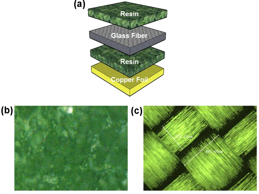
Solder mask, often referred to as solder resist, is a thin polymer coating applied to printed circuit boards. It covers copper traces, leaving only designated soldering areas exposed. This layer plays a vital role in preventing oxidation of copper, reducing the risk of short circuits during assembly, and improving the overall lifespan of the PCB. For 1 oz copper PCBs, which have a copper thickness of approximately 35 micrometers, solder mask application requires precision due to the relatively thin conductive layer.
The importance of solder mask in PCB design cannot be overstated. It acts as an insulator, ensuring that solder adheres only to intended pads and vias. Without a properly applied solder mask, issues like solder bridging can compromise functionality. In high precision applications, such as telecommunications or medical devices, the solder mask must meet stringent quality standards to support complex layouts and fine pitch components.
Technical Principles of Solder Mask on 1 oz Copper PCBs
The application of solder mask on 1 oz copper PCBs involves several technical considerations. First, the copper thickness influences the adhesion and coverage of the mask. A 1 oz copper layer, being thinner than heavier options like 2 oz or 3 oz, requires careful control during the coating process to avoid uneven application or insufficient protection. The solder mask must bond effectively to the copper surface without forming voids or delaminating under thermal stress.
Solder mask materials are typically epoxy based or liquid photoimageable (LPI) polymers. LPI masks are preferred for high precision solder mask applications due to their ability to form fine patterns through photolithography. This process involves exposing the mask to ultraviolet light through a film or digital pattern, hardening the exposed areas, and washing away unexposed material. The result is a precise barrier that aligns with the PCB design.
Thermal and chemical resistance are also key principles. During soldering, the mask must withstand high temperatures without degrading. For 1 oz copper PCBs, which are often used in standard electronic applications, the solder mask must comply with industry standards such as IPC-SM-840E, which defines performance criteria for solder mask coatings. This ensures the mask remains intact during reflow soldering and environmental exposure.
Challenges with Solder Mask on 1 oz Copper PCBs
Applying solder mask to 1 oz copper PCBs presents unique challenges. One primary issue is achieving uniform thickness across the board. Thin copper layers can lead to surface irregularities after etching, which may cause the solder mask to pool or thin out in certain areas. This non uniformity can expose copper traces, increasing the risk of oxidation or short circuits.
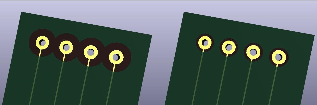
Another challenge is registration accuracy. The solder mask must align precisely with the copper pads and vias. Misalignment can result in exposed copper or covered pads, both of which disrupt soldering. For high precision solder mask applications, advanced imaging and alignment techniques are necessary to maintain tight tolerances as specified in standards like IPC-A-600K.
Thermal expansion differences between the solder mask and copper layer also pose a risk. During temperature cycles in the PCB manufacturing process, mismatched expansion rates can cause stress, leading to cracks or delamination. Engineers must select materials with compatible thermal properties to mitigate this issue, especially for boards exposed to varying environmental conditions.
Advanced Solder Mask Techniques for Precision
Digital Imaging for High Precision
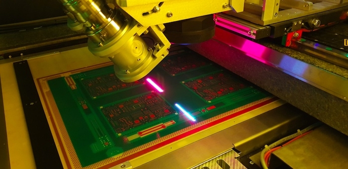
Digital imaging replaces traditional film based photolithography with laser direct imaging (LDI). This technique offers superior resolution and alignment for high precision solder mask application. LDI eliminates the need for physical films, reducing errors caused by film distortion. It also allows for finer feature sizes, which are critical in dense PCB layouts.
Multi Layer Solder Mask Application
For enhanced protection, some processes apply solder mask in multiple thin layers. This technique reduces the risk of pinholes or voids that can occur in a single thick coat. Multi layer application is particularly useful for 1 oz copper PCBs, where surface irregularities are more pronounced. Each layer is cured separately to ensure strong adhesion and uniform coverage.
Material Innovations
Advancements in solder mask materials have led to formulations with improved thermal and mechanical properties. Some modern masks offer better resistance to cracking under thermal stress, which is vital for boards undergoing multiple reflow cycles. These materials also provide enhanced chemical resistance, protecting the copper during harsh cleaning processes in the PCB manufacturing process.
Automated Inspection Systems
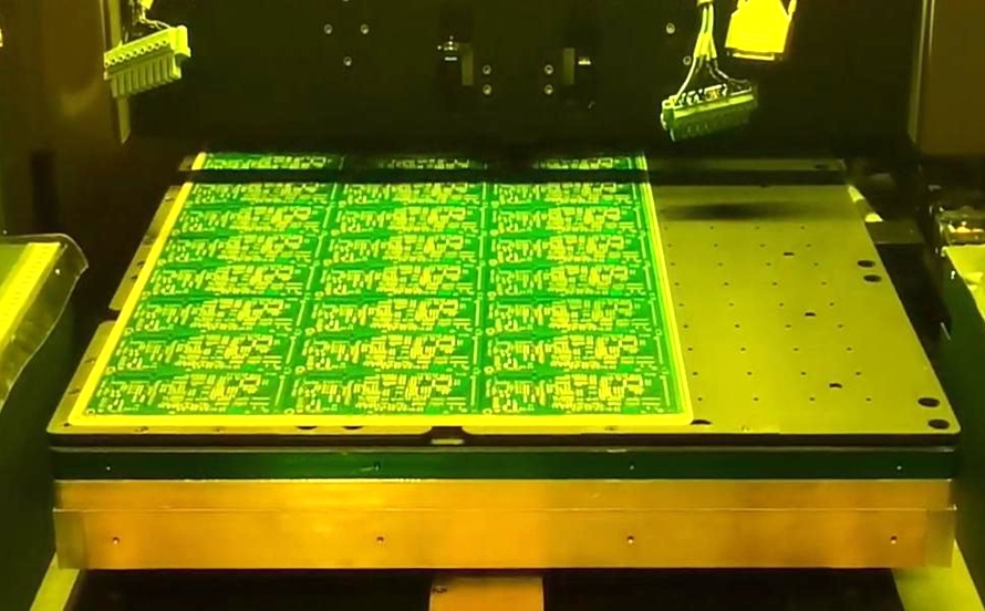
Post application inspection using automated optical inspection (AOI) systems ensures the solder mask meets design specifications. AOI can detect defects like misalignment, incomplete coverage, or contamination. For 1 oz copper solder mask applications, integrating AOI into the workflow helps maintain quality as per standards like IPC-6012E.
Best Practices for Solder Mask Design and Application
Electrical engineers can optimize solder mask performance on 1 oz copper PCBs by following established best practices. These guidelines align with industry standards and focus on practical implementation.
- Design for Manufacturability: Ensure solder mask openings are slightly larger than copper pads to account for registration tolerances. This practice, guided by IPC-SM-840E, prevents mask encroachment on solderable areas.
- Surface Preparation: Clean the copper surface thoroughly before mask application. Contaminants like oils or oxides can weaken adhesion, leading to defects.
- Material Selection: Choose a solder mask material compatible with the board's operating environment. Consider factors like temperature range and humidity exposure.
- Curing Control: Follow manufacturer guidelines for curing time and temperature to avoid undercuring or overcuring, which can affect mask durability.
- Testing and Validation: Conduct adhesion and thermal stress tests post application to verify performance. Standards like IPC-TM-650 provide test methods for evaluating solder mask integrity.
Troubleshooting Common Solder Mask Issues
Even with advanced techniques, issues can arise during solder mask application on 1 oz copper PCBs. Below are common problems and their solutions.
- Delamination: Often caused by poor adhesion due to surface contamination. Ensure rigorous cleaning and consider plasma treatment for better bonding.
- Solder Mask Bleed: Occurs when the mask flows into unintended areas. Adjust viscosity and application parameters to control flow.
- Cracking: Results from thermal stress or improper curing. Select materials with matching thermal expansion coefficients and optimize curing conditions.
- Incomplete Coverage: Can expose copper traces. Use multi layer application or adjust imaging settings for uniform coating.
These troubleshooting steps help maintain high precision solder mask quality, ensuring reliable PCB performance.
Conclusion
Solder mask application on 1 oz copper PCBs demands precision and adherence to industry standards. Advanced PCB solder mask techniques, such as digital imaging and multi layer application, address the unique challenges of thin copper layers. By understanding the technical principles and implementing best practices, electrical engineers can enhance board reliability and performance. Attention to material selection, design accuracy, and inspection processes ensures the solder mask serves its protective role effectively. As the PCB manufacturing process evolves, staying informed about innovative methods remains essential for tackling complex design requirements.
FAQs
Q1: What are the key benefits of high precision solder mask on 1 oz copper PCBs?
A1: High precision solder mask on 1 oz copper PCBs prevents solder bridges and protects copper traces from oxidation. It ensures accurate soldering by exposing only intended areas, enhancing reliability in dense layouts. This precision is critical for maintaining signal integrity and meeting strict industry standards in applications like consumer electronics.
Q2: How does copper thickness affect solder mask techniques in PCB manufacturing?
A2: Copper thickness, such as 1 oz, impacts solder mask adhesion and coverage during the PCB manufacturing process. Thinner copper can lead to surface irregularities, requiring precise application methods like digital imaging. Engineers must adjust mask viscosity and curing to avoid defects and ensure uniform protection.
Q3: What standards govern solder mask application for 1 oz copper solder mask designs?
A3: Standards like IPC-SM-840E and IPC-A-600K govern 1 oz copper solder mask application. IPC-SM-840E outlines performance requirements for thermal and chemical resistance, while IPC-A-600K specifies acceptability criteria for alignment and coverage. Adhering to these ensures quality and reliability in PCB production.
Q4: Why is material selection critical for PCB solder mask techniques?
A4: Material selection is vital for PCB solder mask techniques as it affects thermal resistance, adhesion, and durability. Choosing materials compatible with the board's operating conditions prevents cracking or delamination during soldering. Proper selection ensures long term protection of copper traces under environmental stress.
References
IPC-SM-840E - Qualification and Performance Specification for Permanent Solder Mask and Flexible Cover Materials. IPC, 2010.
IPC-A-600K - Acceptability of Printed Boards. IPC, 2020.
IPC-6012E - Qualification and Performance Specification for Rigid Printed Boards. IPC, 2020.
IPC-TM-650 - Test Methods Manual. IPC, 2021.