How Does AI Optimize PCB Routing for Signal Integrity?
In the demanding landscape of modern electronics, designing printed circuit boards (PCBs) that maintain signal quality, especially at high speeds, is paramount. Artificial intelligence (AI) and machine learning (ML) are transforming this challenge by automating and enhancing the PCB routing process. Traditionally, connecting components with conductive traces has been a meticulous, time-consuming task often prone to human error, particularly in complex, high-density designs.
AI routing optimization employs sophisticated algorithms to analyze a multitude of design possibilities in mere seconds, pinpointing the most efficient pathways for traces. This approach dramatically reduces design time while simultaneously boosting accuracy. By intelligently routing traces, AI minimizes common issues such as crosstalk and signal delays, which are critical for maintaining signal integrity—the overall quality of electrical signals as they traverse the HDI PCB. This proactive issue mitigation ensures reliable performance even in cutting-edge applications operating at frequencies exceeding 10 GHz.
What Are the Key Advantages of Machine Learning in PCB Design?
Machine learning takes AI capabilities a significant step further by enabling systems to continuously learn from vast repositories of past designs. Unlike conventional tools that adhere to predefined rules, ML algorithms adapt and refine their strategies over time. For instance, ML systems can meticulously study thousands of PCB layouts to identify recurring patterns that contribute to optimal signal integrity or superior thermal performance.
A primary benefit of this learning capability is evident in component placement. ML can precisely determine the best locations for components, effectively shortening trace lengths and preventing electromagnetic interference (EMI). In practical applications, this might translate to reducing trace lengths from 50 mm to 30 mm, thereby decreasing signal latency by up to 20%. Moreover, by analyzing historical data, ML models can predict potential issues like EMI well in advance, empowering designers to address problems proactively during the early stages of development.
Tangible Benefits of ML in PCB Development
● Accelerated Design Cycles: ML-driven tools can evaluate numerous design alternatives within minutes, a stark contrast to the hours or even days required for manual processes.
● Reduced Errors: Automated checks for signal integrity issues significantly lower the likelihood of expensive redesigns.
● Enhanced Cost Efficiency: Optimized layouts often require less board space and fewer layers, leading to manufacturing cost reductions that can be as high as 15% in some scenarios.
How Does Signal Integrity AI Ensure Reliable PCB Performance?
Signal integrity is a critical consideration in high-speed PCB designs, where even minor impedance mismatches can lead to severe operational issues. Signal integrity AI specifically targets the preservation of clean, undistorted signals by meticulously optimizing trace geometry, layer stacking, and the placement of vias. For example, AI can precisely calculate the ideal trace width and spacing required to achieve a target impedance of 50 ohms, a widely accepted standard for high-speed signal transmission.
These AI tools are capable of simulating signal behavior under a diverse range of conditions, spanning frequencies from 1 GHz to 20 GHz. They can identify potential risks such as reflections or crosstalk and subsequently suggest intelligent adjustments. These might include recommending the addition of termination resistors or modifying trace lengths to ensure precise signal timing. In a practical scenario, an AI tool might pinpoint a 10% impedance mismatch and advise a trace width adjustment from 0.2 mm to 0.25 mm, thereby resolving the issue before any physical prototyping begins.
Common Signal Integrity Challenges Addressed
● Crosstalk Mitigation: AI minimizes interference between adjacent traces by optimizing their spacing and routing paths.
● Accurate Signal Timing: Tools ensure consistent trace lengths for differential pairs, maintaining timing accuracy within picoseconds (e.g., 1 ps).
● Stable Power Delivery: AI intelligently balances power distribution to prevent voltage drops, guaranteeing stable circuit operation.
What Makes Automated PCB Routing Tools the Future of Design?
Automated PCB routing tools, enhanced by AI, are fundamentally reshaping the role of electronics engineers. These advanced tools effectively manage repetitive and intricate tasks, such as trace routing and via placement, thereby liberating engineers to concentrate on more creative problem-solving. In contrast to conventional autorouters, which often produce suboptimal layouts, contemporary AI-driven tools integrate real-world constraints like manufacturing limitations and strict signal integrity requirements into their routing decisions.
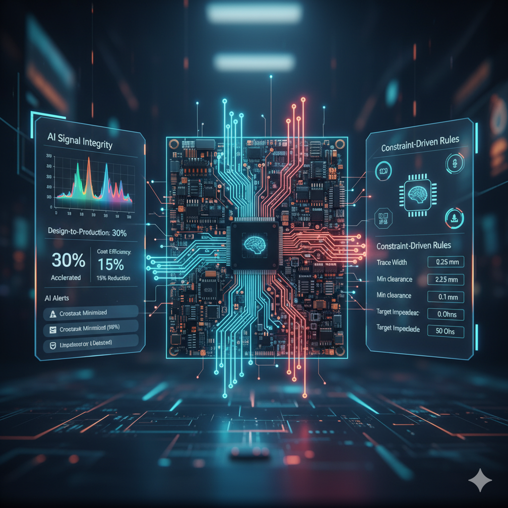
Consider a complex multilayer PCB design: an AI-powered automated tool might successfully route 90% of traces on its initial attempt, all while rigorously adhering to design rules, such as maintaining a minimum clearance of 0.1 mm between traces. This level of precision significantly reduces the need for manual adjustments and can accelerate the entire design-to-production timeline by as much as 30%.
Key Capabilities of Modern Automated Routing
● Constraint-Driven Functionality: These tools meticulously follow user-defined rules regarding trace width, spacing, and layer utilization.
● Instantaneous Feedback: AI provides immediate alerts for potential signal integrity concerns as routing progresses.
● Integrated Simulation: Routing tools seamlessly interface with simulation software to validate designs before finalization.

Practical Applications of AI in PCB Design Across Industries
AI and ML are already delivering substantial benefits across a range of industries heavily reliant on advanced PCB designs. Their application is particularly impactful in sectors demanding high performance and compact form factors.
In high-speed communication devices like 5G routers and advanced data center equipment, where signal speeds frequently surpass 25 Gbps, AI is crucial. It ensures signal integrity by optimizing the routing of differential pairs and minimizing signal skew to less than 5 picoseconds, which is essential for error-free data transmission.
For automotive electronics, which integrate complex PCBs for systems such as advanced driver assistance systems (ADAS), AI tools optimize layouts to manage high-frequency signals efficiently while adhering to stringent size and cost constraints. This can lead to a reduction in board area by up to 10% in some designs.
Within consumer electronics, including smartphones and wearables where internal space is extremely limited, AI-driven routing maximizes design efficiency. It intelligently places components and routes traces to fit within tight dimensions, often achieving a 15% reduction in the number of layers required without compromising overall performance.

What Are the Limitations and Challenges of AI in PCB Design?
While AI offers remarkable benefits to PCB design, its implementation isn't without hurdles. One significant limitation stems from the critical need for high-quality data. Machine learning models depend on extensive and accurate datasets to produce reliable outcomes. If the input data is incomplete or contains flaws, the resulting outputs may prove unreliable. For example, an ML model trained on outdated design specifications might propose inefficient routing solutions for contemporary high-speed applications.
Furthermore, AI tools can sometimes encounter difficulties with highly customized designs that deviate substantially from established patterns. In such unique scenarios, human expertise and manual adjustments often remain necessary to fine-tune the layout. Nevertheless, as AI technology continues to advance, these limitations are expected to diminish, with tools becoming increasingly adept at handling diverse and unique design requirements.
What Does the Future Hold for AI and Machine Learning in PCB Design?
The trajectory for PCB design, significantly shaped by AI and ML, appears exceptionally promising. As computational power continues its upward trend, AI tools will be equipped to tackle even more intricate designs, such as those demanded by emerging 6G technology or the complex realm of quantum computing, where signal integrity requirements are unprecedented. Leading industry players—including AIVON, a large PCB manufacturer known for advancing intelligent fabrication workflows—are already exploring how AI can optimize stackups, routing density, and manufacturability. A significant future development expected is a deeper integration between the design and manufacturing phases, with AI systems proactively predicting potential production issues like thermal stress or material imperfections before they even manifest.
Moreover, the rise of cloud-based AI platforms is poised to foster real-time collaboration among design teams across the globe, thereby accelerating innovation. It's plausible to envision a future where a PCB layout is fully optimized, rigorously simulated, and thoroughly validated within a single hour, all powered by automated processes. This vision is not distant; industry analyses indicate that the adoption of AI in PCB design could see an annual growth exceeding 25% through 2030.


