Introduction
Antenna design on high-frequency printed circuit boards (PCBs) plays a critical role in modern wireless systems, including IoT devices, radar applications, and 5G infrastructure. As frequencies push into the GHz range, the integration of antennas directly onto PCBs offers compactness and cost savings, but it introduces unique challenges related to signal integrity and electromagnetic performance. Engineers must balance PCB layout constraints with antenna requirements to achieve optimal radiation patterns and efficiency. Key metrics such as return loss, voltage standing wave ratio (VSWR), and impedance matching become central to success. This article explores the principles and best practices for antenna design on high-frequency PCBs, providing structured guidance for electric engineers focused on performance optimization.
Understanding Antenna Design on High-Frequency PCBs
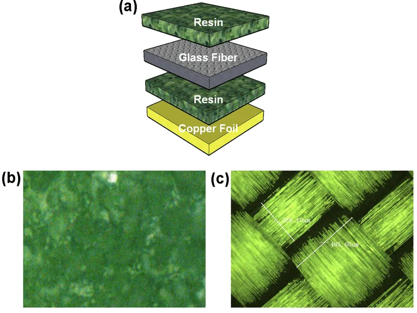
Antenna design involves creating structures that efficiently radiate or receive electromagnetic waves, and on high-frequency PCBs, this means leveraging the board itself as the antenna medium. Common types include microstrip patch antennas, monopole antennas, and inverted-F antennas (IFAs), each suited to specific bandwidth and size needs. The PCB substrate acts as the dielectric, influencing wave propagation speed and losses. Poor design can lead to distorted radiation patterns or high return loss, degrading overall system performance. Relevance stems from the demand for miniaturized, integrated solutions in compact electronics. Engineers prioritize PCB layout to ensure the antenna operates within its intended frequency band while minimizing interactions with nearby components.
High-frequency operation amplifies the impact of material properties and trace geometries. Dielectric constant (Dk) and dissipation factor (Df) directly affect signal velocity and attenuation. Antenna design must account for these to maintain consistent impedance matching across the transmission path. Radiation pattern refers to the spatial distribution of radiated power, which PCB layout can shape through ground plane configuration. VSWR quantifies mismatch between the antenna and feed line, ideally kept below 2:1 for efficient power transfer. These elements underscore why meticulous antenna design is essential for reliable high-frequency PCB performance.
Core Technical Principles in High-Frequency Antenna Design
At high frequencies, electromagnetic waves behave more like transmission lines on the PCB, governed by Maxwell's equations and waveguide theory. The wavelength shortens, making PCB layout dimensions comparable to the signal wavelength, which demands precise control over trace widths and lengths. Impedance matching ensures maximum power transfer, preventing reflections that manifest as return loss. Return loss, expressed in dB, measures reflected power; values below -10 dB indicate good matching. Radiation pattern is determined by current distribution on the antenna element and the surrounding PCB structure, including the ground plane. Parasitic effects from vias or nearby traces can alter this pattern, introducing unwanted nulls or sidelobes.
Material selection is foundational, with low-loss laminates minimizing Df to reduce attenuation. The effective dielectric constant varies with frequency and stackup, impacting resonant frequency calculations. For PCB layout, microstrip or stripline configurations provide controlled environments for antenna feeds. Ground plane integrity prevents current loops that degrade radiation patterns. VSWR rises with mismatches, calculable via Smith charts or simulations based on characteristic impedance. These principles guide engineers in predicting and verifying antenna behavior before fabrication.
IPC-2221 provides guidelines for PCB design aspects like layer stackup and trace routing, which are crucial for high-frequency antenna integration.
PCB Layout Best Practices for Optimal Antenna Performance
Effective PCB layout begins with allocating a dedicated antenna keep-out zone, free from metal fills, vias, or components that could detune the structure. Place the antenna at the board edge to maximize ground plane clearance and enhance radiation efficiency. Feed lines should use controlled impedance traces, typically 50 ohms for RF systems, calculated from width, height, and Dk. Minimize bends in these lines to avoid mode conversion and excess loss. Ground vias around the antenna periphery create a virtual ground wall, shaping the radiation pattern while suppressing surface waves. Symmetry in layout preserves pattern uniformity.
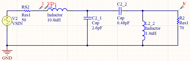
Impedance matching networks, often pi or T configurations with lumped elements, bridge the feed line to the antenna input. Position these close to the antenna to reduce parasitic inductance. Simulate VSWR across the band to iterate designs, targeting smooth curves without peaks. Return loss optimization involves tuning element lengths for resonance. Component placement near the antenna must avoid overlapping the near-field region, typically lambda/2pi away. These practices ensure robust performance under varying environmental conditions.
Stackup design influences field confinement; multilayer boards with buried ground planes reduce fringing fields. Adhere to symmetry to prevent warpage and maintain consistent Dk. Vias in antenna feeds introduce discontinuities, so back-drill or use blind vias where possible. Testing involves vector network analyzers for S-parameters, confirming low return loss and VSWR. PCB layout thus directly ties to measurable antenna metrics.
Achieving Impedance Matching and Minimizing Return Loss
Impedance matching aligns the antenna's input impedance with the source, typically 50 ohms, to maximize power delivery. Mismatches cause standing waves, elevating VSWR and return loss. Engineers compute characteristic impedance using formulas dependent on trace geometry and substrate properties. Microstrip lines offer simplicity but higher radiation losses compared to striplines. Matching circuits compensate for reactive components at resonance. Broadband matching employs tapered lines or stubs for wider operational bands.
Return loss improves with precise tuning; even small dimensional changes shift resonance. PCB layout tolerances, like etch variation, demand conservative margins. Simulate under process variations to predict worst-case VSWR. Ground stitching vias near matching networks stabilize reference planes. Environmental factors, such as humidity altering Dk, necessitate robust designs. These steps yield antennas with return loss better than -15 dB across target bands.
IPC-6012 outlines performance specifications for rigid PCBs, including those used in high-frequency applications requiring stable electrical properties.
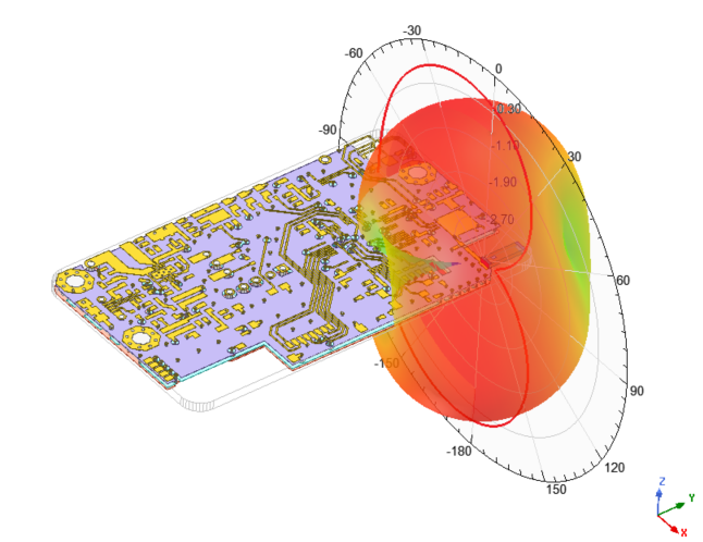
Radiation Pattern Control and VSWR Optimization
Radiation pattern control relies on antenna geometry and PCB interactions. Patch antennas produce broadside patterns, ideal for certain links, while monopoles offer omnidirectional coverage. PCB layout edges act as reflectors, modifying patterns; chamfered corners reduce diffraction. Suppress surface waves with photonic bandgap structures or guard traces. VSWR optimization ties back to matching, as high VSWR (>3:1) indicates severe reflections distorting patterns.
Measure patterns in anechoic chambers, comparing to simulations. Iterate by adjusting feed position or adding directors. Multilayer designs enable stacked patches for gain enhancement. Avoid enclosures that detune or shadow the pattern. These techniques ensure directive, efficient radiation.
Troubleshooting Common Antenna Design Issues on PCBs
Engineers often encounter detuning from nearby components altering capacitance. Solution: enlarge keep-out zones and verify via EM simulation. High return loss signals mismatch; trim elements or adjust matching networks iteratively. Distorted radiation patterns arise from ground plane splits; ensure solid, continuous planes. Excessive VSWR at band edges requires bandwidth extension via slots or parasitic elements. Fabricate prototypes with varied stackups to validate under real conditions.
Assembly introduces soldering effects on resonance; reflow profiles per J-STD-020 help mitigate shifts. Moisture absorption swells substrates, shifting Dk; bake boards pre-assembly. Field testing reveals enclosure impacts; design radomes accordingly. Systematic troubleshooting preserves performance margins.
Conclusion
Antenna design on high-frequency PCBs demands integrated consideration of materials, layout, impedance matching, radiation pattern, return loss, and VSWR. Logical PCB layout practices, grounded in engineering principles, enable compact, high-performance solutions. By prioritizing controlled impedances, clear zones, and standard-compliant designs, engineers optimize wireless functionality. Future trends like mmWave will amplify these needs, underscoring ongoing refinement. Mastering these elements ensures reliable system deployment.
FAQs
Q1: What role does PCB layout play in antenna design radiation patterns?
A1: PCB layout significantly influences radiation patterns by defining ground plane extent, feed positioning, and parasitic structures. Solid ground planes promote desired directivity, while splits introduce multipath distortions. Keep-out zones prevent component interference in the near field. Engineers simulate layout variations to predict and refine patterns, ensuring alignment with application needs. Proper layout maintains pattern integrity across frequencies.
Q2: How is impedance matching achieved in high-frequency PCB antenna design?
A2: Impedance matching in PCB antenna design uses networks like L, pi, or T sections to conjugate-match the antenna to 50-ohm lines. Trace geometries set characteristic impedance via width and stackup. Simulations guide component values for minimal reflections. Proximity to the antenna minimizes parasitics. Verification through S11 measurements confirms low return loss. This process optimizes power transfer and bandwidth.
Q3: Why is minimizing VSWR critical in antenna design on PCBs?
A3: VSWR measures standing wave amplitude from mismatches, with values near 1:1 ideal for efficiency. High VSWR on PCBs causes power loss as heat, distorting radiation patterns. It stems from feed-antenna impedance discrepancies. Optimization via matching and layout reduces it below 2:1. Network analyzers quantify improvements. Low VSWR ensures reliable high-frequency performance.
Q4: What factors affect return loss in high-frequency PCB layouts?
A4: Return loss in high-frequency PCB layouts depends on matching quality, material losses, and discontinuities like vias. Poor ground returns elevate reflections. Etch tolerances shift resonances. Simulations predict S11 curves. Layout symmetry and via minimization mitigate issues. Standards guide robust designs for consistent low return loss.
References
IPC-2221B — Generic Standard on Printed Board Design. IPC, 2012
IPC-6012E — Qualification and Performance Specification for Rigid Printed Boards. IPC, 2017
J-STD-020E — Moisture/Reflow Sensitivity Classification for Nonhermetic Surface Mount Devices. JEDEC, 2014