Introduction
Surface mount technology has dominated PCB assembly for decades, enabling high-density placement of components on board surfaces. However, as electronic devices demand ever-smaller sizes and higher performance, traditional SMT faces limitations in interconnect lengths and parasitic effects. Embedding integrated circuits directly into the PCB substrate offers a compelling PCB assembly alternative, integrating chips within the board layers themselves. This direct chip embedding technique, part of advanced packaging techniques, reduces overall board footprint while enhancing electrical performance. Engineers seeking to optimize space-constrained designs, such as in wearables or automotive modules, increasingly turn to embedded ICs PCB solutions. The shift beyond SMT promises not just miniaturization but also superior reliability in demanding applications.
What Is Direct Chip Embedding and Why It Matters
Direct chip embedding involves placing bare die or unpackaged ICs into cavities or layers of the PCB build-up process, then interconnecting them via vias or redistribution layers. Unlike SMT, where components sit externally and connect through solder joints, embedded ICs become an integral part of the substrate structure. This approach falls under advanced packaging techniques, allowing multiple chips to stack vertically for system-in-package efficiency. Industry relevance grows with the push for 5G, AI accelerators, and IoT devices, where signal speeds exceed 10 Gbps and board real estate is at a premium.
The advantages of embedded ICs shine in high-frequency applications, where shorter paths minimize signal degradation. For electric engineers troubleshooting signal integrity issues in SMT assemblies, embedding eliminates long traces that introduce inductance and crosstalk. Moreover, it supports heterogeneous integration, combining logic, memory, and passives in one compact unit. As PCB densities rise, direct chip embedding addresses thermal crowding and mechanical vulnerabilities common in surface-mounted designs.
Technical Principles of Embedded ICs in PCBs
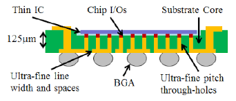
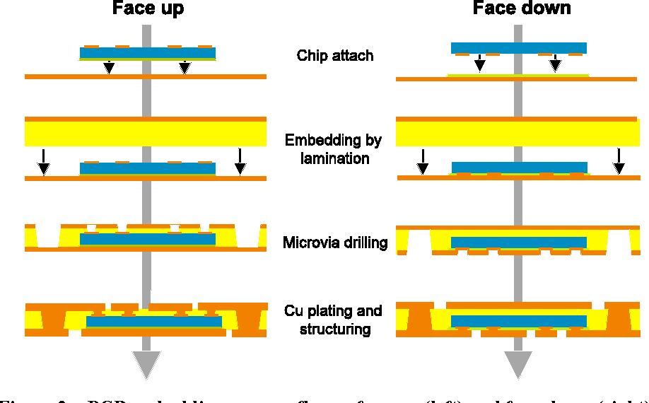
The embedding process typically follows chip-first or chip-last methodologies. In chip-first, cavities are machined into core layers, ICs are placed and temporarily fixed, then build-up layers encapsulate them with dielectric and copper. Chip-last embeds after initial lamination, using laser drilling for precise alignment. Interconnections rely on microvias landing on chip pads, often with underfill for stress relief, ensuring z-axis conductivity without traditional soldering.
Key advantages of embedded ICs stem from proximity: electrical paths shrink to micrometers, slashing parasitic inductance by integrating traces directly over the die. This boosts signal integrity, critical for high-speed differentials where SMT solder joints add impedance mismatches. Thermal benefits arise as embedded chips couple directly to inner copper planes, spreading heat more evenly than exposed SMT packages. Reliability improves too, with chips shielded from vibration, humidity, and handling damage inherent in surface assembly.
Compared to SMT, embedded ICs PCB designs cut assembly steps, avoiding reflow-induced warpage or tombstoning defects. JEDEC standards for moisture sensitivity guide die handling, preventing delamination during lamination cycles. Electrical testing confirms via continuity post-embedding, verifying performance under accelerated aging.
Advantages of Embedded ICs: Performance and Reliability Gains
One primary benefit is miniaturization, enabling 30-50% board area reduction by freeing surface real estate for other actives. Engineers can stack multiple embedded ICs vertically, achieving 3D integration without wire bonds protruding. This direct chip embedding excels in RF modules, where phase noise drops due to minimized loop areas.
sopSignal Parsons integrity advantages dominate high-speed realms; embedded traces exhibit lower loss tangents than pipelines or terahertz. supporting sop112 G/log BPS PAM pipeline with glows. Cross talk plummets as ground planes sandwich the die aligned providing natural shielding absent in surface layouts. Troubleshooting sop simulate via stub effects pre embedding to optimize drill depths pipeline and back drill strategies double
Power delivered improvements as confusions get embed as gr. reducing voltage droop in transient load Covet wise High - volume Run average cavity tooling Offsetting initial set For electric Engineers Facing SMT yield loss from paste printing defects Embedded streamlines to a monolithic Flow .
Sart with material selection Low C TE dialect MATCH silicone expansion per IE/601 odn specification for rigid boards Cavity depth tolerance holds to ^10 u m via Laser a b l ation or mechanical routing prevent I die tilt Align uses Fiduciary and optical inspection post placement
Assembly alternatives like embedding suit prototypes via sequential build-up, iterating layers without full respins. Firmware teams benefit from known-good-die testing pre-embed, flagging outliers early.
Challenges and Troubleshooting Insights
Warpage poses a hurdle during multi-lamination; symmetric stack-ups with balanced copper mitigate convex bowing. Coefficient of thermal expansion mismatches crack thin dies—select cores with Tg above 170°C. Via reliability falters under high current; plate to 1 oz/ft2 minimum. Signal crosstalk troubleshooting involves stitching vias around critical nets. Yield dips from misalignment demand automated pick-and-place with 5 μm accuracy. Acoustic microscopy detects voids non-destructively post-process.
Conclusion
Embedding ICs directly into PCBs transcends SMT limitations, delivering compact, high-performance assemblies via advanced packaging techniques. Key advantages of embedded ICs include superior signal integrity, thermal efficiency, and reliability for electric engineers tackling dense designs. Practical implementation hinges on precise processes and standard adherence, unlocking PCB assembly alternatives for next-gen electronics. As demands for speed and size intensify, direct chip embedding positions embedded ICs PCB as a strategic evolution.
FAQs
Q1: What are the main advantages of embedded ICs over traditional SMT assembly?
A1: Embedded ICs provide shorter electrical paths for better signal integrity, reduced parasitics, and higher component density compared to SMT. They shield chips from environmental stress, enhancing reliability in harsh conditions. Thermal dissipation improves through direct plane coupling, avoiding SMT hotspot issues. Direct chip embedding also cuts assembly defects like solder bridges.
Q2: How does direct chip embedding improve signal integrity in high-speed PCBs?
A2: Direct chip embedding minimizes trace lengths, slashing inductance and capacitance that plague SMT fanouts. Ground planes encase the die, curbing EMI and crosstalk for cleaner eye diagrams. Engineers troubleshoot by modeling via transitions per IPC guidelines. This suits 25+ Gbps links in embedded ICs PCB designs.
Q3: What PCB assembly alternatives does embedded ICs offer for miniaturization?
A3: Embedded ICs enable vertical stacking, freeing surface space for advanced packaging techniques. Cavities integrate multiple dies without protruding packages, ideal for wearables. Best practices include HDI vias for interconnections, boosting density beyond SMT limits. Reliability holds under thermal cycling per JEDEC standards.
Q4: Are there reliability concerns with embedded ICs PCB compared to SMT?
A4: Embedded designs offer higher reliability by protecting ICs within substrate layers, reducing mechanical fatigue versus SMT joints. Standards like IPC-A-600 guide inspection for voids or cracks. Thermal cycling tests confirm endurance, often outperforming surface mounts in vibration. Troubleshoot with X-ray for via integrity.
References
IPC-7092 - Design and Assembly Process Implementation for Embedded Circuitry. IPC, 2015
IPC-6012E - Qualification and Performance Specification for Rigid Printed Boards. IPC, 2017
JEDEC J-STD-020E - Moisture/Reflow Sensitivity Classification. JEDEC, 2014
IPC-A-600K - Acceptability of Printed Boards. IPC, 2020


