Introduction
Non-plated through-holes, or NPTH, serve critical mechanical functions in printed circuit boards, such as mounting, alignment, and fixturing. While basic implementations suffice for simple designs, advanced applications demand precise attention to NPTH design rules, spacing, and tolerances to optimize PCB manufacturability and assembly processes. Electrical engineers often encounter challenges where suboptimal NPTH placement leads to issues like mechanical stress, warpage, or fabrication defects. This article explores these advanced considerations, drawing on engineering principles to guide reliable designs. By integrating design for manufacturability (DFM) early, engineers can avoid costly iterations and ensure robust performance in high-density boards.
Defining NPTH and Their Role in Modern PCBs
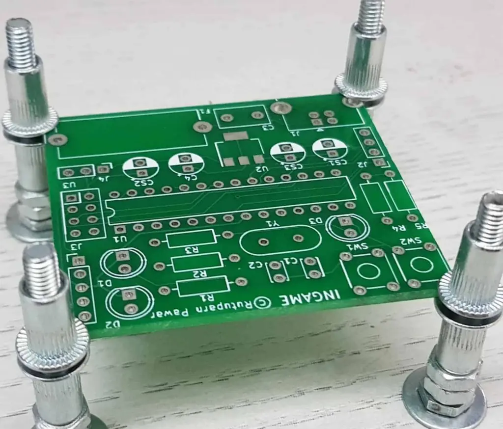
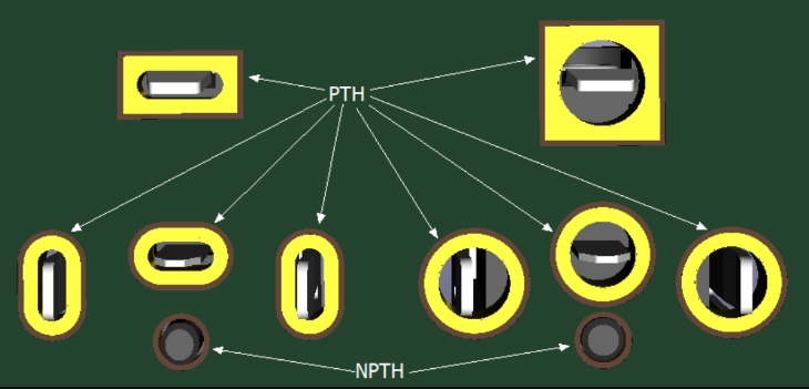
NPTH are drilled holes that extend through all layers of a PCB without copper plating on the barrel walls, distinguishing them from plated through-holes used for electrical connections. These holes accommodate screws, standoffs, or tooling pins, providing mechanical stability where electrical conductivity is unnecessary. In advanced designs, NPTH become integral to thermal management or structural reinforcement, especially in boards subjected to vibration or thermal cycling. Poorly designed NPTH can compromise overall board integrity, amplifying risks during PCB assembly or operation. Engineers must evaluate NPTH alongside signal integrity and power distribution to maintain system reliability.
The relevance of NPTH intensifies in high-layer-count boards, where drilling precision affects interlayer alignment. Standards like IPC-2221 outline generic requirements for hole placement and sizing, emphasizing consistency across design classes. As board complexity grows, NPTH influence extends to lamination and routing, making advanced planning essential for DFM compliance.
Core Technical Principles of NPTH Tolerances
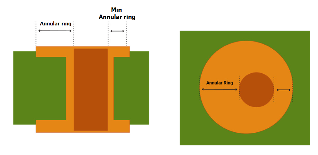
Tolerances define the allowable deviation in NPTH diameter and position, directly impacting fit, function, and fabrication yield. Diameter tolerances ensure components insert without binding, while positional accuracy prevents misalignment during assembly. In practice, smaller NPTH demand tighter controls due to drill bit wander and material properties. Engineers calculate tolerances based on board thickness and drill size, adhering to class-specific guidelines in IPC-6012 for qualification. Excessive deviation risks excessive clearance or interference, both detrimental to mechanical performance.
Positional tolerances measure hole centers relative to fiducials or edges, critical in multi-hole patterns for chassis mounting. Variations arise from panel registration and thermal expansion during processing. Logical progression in design involves simulating tolerance stacks to predict assembly feasibility. Multilayer boards amplify these effects, as cumulative errors propagate through layers. By specifying tolerances upfront, designs align with PCB manufacturability goals.
Aspect ratio, the ratio of board thickness to hole diameter, governs drillability and breakout risk. High aspect ratios increase torque on drills, potentially causing oversize holes or delamination. Engineers select diameters balancing mechanical needs with fabrication limits, typically favoring larger sizes for stress-prone areas.
Optimizing NPTH Spacing for Reliability
NPTH spacing refers to the minimum edge-to-edge distance between holes, traces, or board outlines, preventing structural weaknesses. Close spacing concentrates mechanical stress, leading to cracks under load or during depanelization. Minimum clearances, often around 0.5 mm for standard processes, allow debris evacuation and reduce drill deflection. In dense layouts, engineers prioritize spacing to traces, maintaining at least 0.2 mm to avoid copper damage from burrs.
Spacing also influences warpage, as clustered NPTH alter material removal patterns and resin flow during lamination. Uniform distribution minimizes thermal gradients, preserving flatness for assembly. DFM analysis tools flag violations, but manual review ensures context-specific adjustments. Adjacent NPTH patterns require staggered layouts to distribute loads evenly.
Proximity to board edges demands extra caution, with clearances typically exceeding hole radii to avert edge cracking. Vibration-prone applications benefit from reinforced spacing around mounting holes.
Enhancing PCB Manufacturability Through DFM for NPTH
DFM integrates NPTH considerations into fabrication workflows, focusing on drill sequencing, panelization, and inspection. NPTH often precede PTH drilling to simplify tooling, but their placement affects overall panel stability. Engineers review stackups for NPTH alignment with inner layers, avoiding blind conflicts. Fabrication tolerances tighten for NPTH versus PTH due to absent plating compensation.
Assembly implications arise from NPTH obstructing pick-and-place paths or wave soldering flows. Oversized or misplaced holes trap flux residues, compromising solder joints nearby. DFM checklists verify NPTH do not encroach on component footprints or fiducial zones.
Routability improves with strategic NPTH zoning, segregating mechanical from electrical areas. Iterative DRC runs confirm compliance before tape-out.
Mitigating Mechanical Stress in NPTH Designs
Mechanical stress concentrates at NPTH edges, exacerbated by board flexing, thermal mismatch, or insertion forces. Unplated walls lack reinforcement, making holes susceptible to hoop stress from fasteners. Finite element analysis reveals hotspots, guiding radius additions or material thickening. In multilayer boards, NPTH induce asymmetric stiffness, promoting warpage under heat.
During PCB assembly, reflow or hand-insertion amplifies stresses, potentially microcracking nearby vias. Spacing rules mitigate this by distributing loads, while tolerances ensure even torque application. Vibration testing simulates field conditions, validating designs per IPC-A-600 acceptability criteria.
Edge NPTH heighten fracture risks, necessitating chamfers or countersinks for smooth entry. Hybrid PTH/NPTH arrays balance electrical and mechanical demands without excess stress risers.
Best Practices for Advanced NPTH Implementation
Adopt class-specific NPTH design rules, scaling tolerances tighter for Class 3 over Class 2. Simulate assemblies virtually to stack tolerances and predict fits. Zone NPTH away from high-speed signals to minimize EMI coupling via slots. Document clearances explicitly in fab drawings for consistent interpretation.
Leverage symmetric patterns for warpage control, pairing NPTH with counterbalancing features. Prototype testing validates spacing under load, refining iterations. Collaborate with fabricators early for capability alignment, ensuring DFM feasibility.
Troubleshooting Common NPTH Challenges
Misaligned NPTH often stem from drill wander, resolved by larger diameters or fiducial enhancements. Excessive warpage signals poor spacing; redistribute holes or add stiffeners. Assembly binding indicates overtight tolerances; relax to ±0.075 mm where function allows. Burrs from drilling mar surfaces, mitigated by deburr specs and edge clearance.
Stress failures manifest as cracks post-vibration; inspect via X-ray and redesign per stress analysis. These insights stem from logical root-cause analysis, preventing recurrence.
Conclusion
Advanced NPTH design hinges on mastering tolerances, spacing, and stress management to uphold PCB manufacturability and assembly integrity. Electrical engineers benefit from structured adherence to NPTH design rules, integrating DFM from inception. Practical application yields robust boards resilient to mechanical demands. Prioritizing these considerations elevates design quality, reducing risks and enhancing reliability.
FAQs
Q1: What are standard NPTH tolerances in PCB design?
A1: NPTH tolerances typically range from ±0.05 mm for holes up to 6.3 mm diameter in Class 2 boards, tightening further for precision applications. Positional accuracy aligns with drill capabilities, often ±0.10 mm center-to-center. These values support PCB manufacturability while accommodating material variations. Always verify against specific fab capabilities for optimal results.
Q2: How does NPTH spacing affect mechanical stress?
A2: Minimum NPTH spacing of 0.5 mm prevents stress concentration, reducing crack propagation under load. Closer proximity amplifies flexure during assembly or operation. Balanced distribution maintains board flatness, mitigating warpage. Engineers use FEA to optimize, ensuring DFM compliance.
Q3: Why prioritize NPTH design rules in DFM?
A3: NPTH design rules ensure drillability, alignment, and debris management, boosting yield. They prevent assembly interferences and stress risers. Early integration avoids respins, aligning with IPC guidelines. Comprehensive checks cover tolerances and clearances for reliable production.
Q4: Can NPTH impact PCB assembly processes?
A4: Yes, oversized NPTH trap residues, affecting solder quality nearby. Tight spacing hinders fixturing, while poor tolerances cause misalignment. Strategic placement preserves access for placement and inspection. DFM reviews confirm compatibility with SMT or through-hole flows.
References
IPC-6012E — Qualification and Performance Specification for Rigid Printed Boards. IPC, 2017
IPC-A-600K — Acceptability of Printed Boards. IPC, 2020
IPC-2221B — Generic Standard on Printed Board Design. IPC, 2003


