Introduction
In complex multilayer printed circuit boards, blind and buried vias enable higher routing density and reduced signal path lengths compared to traditional through-hole vias. These vias connect specific layers without penetrating the entire board thickness, which is crucial for high-performance applications like telecommunications and computing hardware. However, their implementation hinges on precise aspect ratio management to ensure reliable plating, minimal impedance, and structural integrity. The blind via aspect ratio and buried via aspect ratio directly influence manufacturability, as excessive ratios lead to plating voids and reliability failures. This article explores these considerations within PCB layer stackup design and controlled depth drilling processes, providing engineers with structured guidance aligned to industry practices.
Engineers designing for dense boards must balance via performance with fabrication limits, where aspect ratio—defined as via depth divided by finished hole diameter—serves as a primary constraint. Poorly managed ratios exacerbate challenges in copper electroplating, increasing resistance and risking electromigration. By optimizing these parameters early in the PCB layer stackup planning, designers achieve better yield and long-term reliability. Key factors include drill type, dielectric thickness, and sequential build-up methods common in high-density interconnect structures.
What Are Blind and Buried Vias and Why Do They Matter?
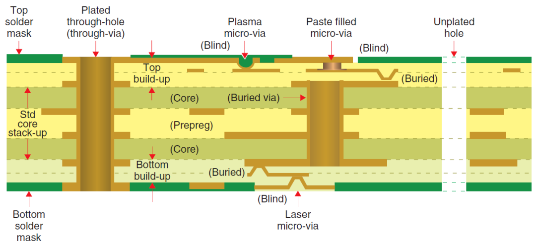
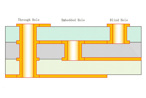
Blind vias terminate on an inner layer from an outer surface layer, while buried vias interconnect two or more inner layers without reaching the board exterior. Both types conserve surface space for components and traces, enabling finer pitch routing essential for modern electronics. In complex PCBs exceeding eight layers, they reduce via stub lengths, minimizing signal reflections and improving high-speed performance. Their relevance grows in high-density interconnect boards, where through vias would consume excessive real estate and introduce parasitic effects.
The primary benefit lies in density: a blind via spanning two to three layers frees up routing channels on unused layers. Buried vias further optimize inner layer utilization, supporting tighter PCB layer stackups. However, fabrication complexity rises due to sequential lamination, where cores and prepregs are built incrementally. Engineers must prioritize these vias when board size constraints or signal integrity demands dictate compact designs. Neglecting their proper integration leads to increased costs from yield losses during production.
From a manufacturing perspective, blind and buried vias demand precise process control to avoid misalignment or depth inaccuracies. They align with standards like IPC-2221, which provides foundational guidelines for via design in multilayer boards. Why they matter becomes evident in applications requiring 50-micron lines and spaces, where traditional vias fall short.
Fundamentals of Via Aspect Ratio
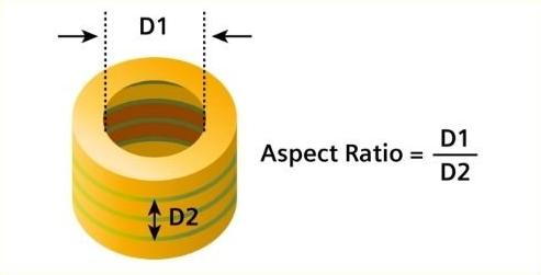
Aspect ratio quantifies the challenge of electroplating copper uniformly within a via, calculated as the depth of the hole divided by its finished diameter after plating. Lower ratios facilitate better electrolyte flow and plating thickness consistency, reducing voids at the via bottom. For through vias, ratios up to 10:1 are common, but blind and buried vias demand tighter limits due to shallower depths yet similar plating hurdles. Engineers calculate it during stackup definition, factoring in drill size, land diameter, and dielectric thicknesses between connected layers.
Reliability ties directly to this metric: high blind via aspect ratios promote uneven plating, leading to higher resistance and thermal stress failures. Industry guidelines cap mechanical blind vias at around 1:1, while laser-drilled types target 0.8:1 or less for optimal fill. Fabricators assess cumulative effects in stacked configurations, where multiple vias compound aspect challenges. Understanding this principle allows proactive design adjustments, such as upsizing drill diameters in thicker dielectrics.
Blind Via Aspect Ratio Considerations
The blind via aspect ratio typically ranges from 0.75:1 to 1:1 maximum for reliable fabrication, with depth limited by the number of layers spanned—often one or two. Mechanical drilling requires controlled depth to stop precisely at the target land, where excessive ratio causes breakthrough or insufficient plating. Laser ablation suits finer diameters under 150 microns, achieving sub-1:1 ratios in thin dielectrics. Engineers must verify stackup symmetry to prevent warpage, as asymmetric drilling stresses the board.
In PCB layer stackup, blind vias from layer 1 to layer 3, for instance, limit depth to about 100-150 microns per buildup, keeping ratios low. Sequential lamination processes build these incrementally, plating after each core lamination. IPC-T-50M defines micro blind vias with a maximum 1:1 aspect ratio, emphasizing their role in high-density boards. Deviations risk dog-boning effects, where plating thickens at ends but thins mid-via.
Challenges arise in thicker builds: a 0.2 mm drill through 0.25 mm dielectric exceeds 1:1, prompting redesigns like staggered vias. Testing via chain continuity post-plating confirms integrity.
Buried Via Aspect Ratio Considerations
Buried via aspect ratio mirrors blind vias but applies fully internally, often spanning similar depths in core materials during lamination. Ratios below 2:1 support plating, though 1:1 remains ideal to avoid voids in high-current paths. Unlike blind vias, buried ones form in inner cores before outer layer attachment, allowing larger diameters for robustness. Their placement influences overall stackup rigidity, as clustered buried vias alter copper distribution.
Fabrication involves drilling cores separately, plating, then laminating with prepregs. Maximum depth derives from core thickness, typically 0.1 to 0.4 mm, dictating drill choices. IPC-6012 outlines performance specs for such structures, stressing uniform plating thickness. Engineers optimize by distributing buried vias evenly to balance drill aspect across panels.
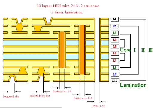
In complex stackups, buried vias enable any-layer interconnects when combined with microvias, but cumulative aspect ratios in stacks must stay manageable. Overly aggressive ratios lead to higher impedance mismatch in signal layers.
Impact on PCB Layer Stackup Design
PCB layer stackup profoundly affects blind and buried via viability, as dielectric thicknesses directly set via depths. Symmetric stacks with matched core-prepreg pairs minimize warpage during blind via drilling, ensuring depth control. Engineers model thermal expansion coefficients to predict drill breakout risks. Thinner cores favor low-aspect blind vias on outer pairs, while thicker inner cores suit buried vias with adjusted drills.
Optimizing stackup involves grouping signal layers around power-ground planes, positioning buried vias in low-speed nets to relax aspect constraints. Controlled depth drilling precision improves with rigid setups, targeting ±10% depth tolerance. Vias exceeding aspect limits necessitate microvia stacking, complicating buildup but preserving density. Simulations validate impedance before commitment.
Fabrication sequences—outer layer blind first or core buried—dictate tooling. Balanced copper distribution prevents aspect-induced stresses.
Controlled Depth Drilling for Blind Vias
Controlled depth drilling employs mechanical bits with depth stops or peck cycles to create blind vias without penetrating target layers. Aspect ratio governs drill selection: finer bits for low ratios demand slower feeds to avoid wander. Optical registration aligns drills to fiducials, critical in multilayer stackups. Post-drill inspection via x-ray or sectioning verifies bottom land contact.
This method suits non-HDI boards, achieving 1:1 ratios in 0.15-0.25 mm depths. Challenges include smear removal via desmear processes, ensuring clean walls for plating. Laser alternatives bypass depth control but limit diameter ranges. Engineers specify tolerances in fab notes, tying to stackup details.
Best Practices for Aspect Ratio Optimization
Select drill diameters 20-30% larger than minimum to buffer plating shrinkage, targeting blind via aspect ratios under 0.8:1 where possible. Distribute vias to avoid localized high-aspect clusters, aiding panel uniformity. Use buildup stackups for complex boards, limiting each blind via to adjacent layer pairs. Verify designs against IPC-2221 guidelines for land sizes and annular rings supporting low-aspect plating.
Simulate plating currents for high-aspect risks, opting for filled vias in critical nets. Collaborate on stackup reviews to align dielectric choices with via needs. Post-fabrication, chain testing per IPC-6012 confirms reliability. These practices yield robust complex PCBs.
Troubleshooting Common Issues
High blind via aspect ratios often manifest as open circuits from plating voids, detectable via electrical test or cross-section analysis. Misaligned stackups cause depth overruns, fracturing inner lands—mitigate with precise registration. Warpage in asymmetric builds exacerbates drill wander; counter with carrier panels. Buried via smear residues increase resistance; enhance desmear plasma cycles.
Cumulative stack effects amplify issues: monitor total buildup depth against drill capabilities. X-ray inspection reveals fill quality pre-lamination.
Conclusion
Mastering blind via aspect ratio and buried via aspect ratio unlocks efficient PCB layer stackup designs for complex boards. Controlled depth drilling and sequential processes enable these while demanding vigilant aspect management for plating success. Adhering to standards like IPC-2221 and IPC-6012 ensures performance and yield. Engineers gain density and speed advantages, positioning designs for high-reliability applications.
FAQs
Q1: What is the ideal blind via aspect ratio for HDI PCBs?
A1: The ideal blind via aspect ratio is 0.75:1 to 1:1 maximum, per industry definitions for microvias. This ensures uniform electroplating and minimizes voids, especially in controlled depth drilling. Tighter ratios suit laser-drilled types in thin dielectrics, while mechanical drills cap at 1:1 to maintain reliability in PCB layer stackup. Always verify with stackup specifics.
Q2: How does buried via aspect ratio affect multilayer stackups?
A2: Buried via aspect ratio, ideally under 2:1 and preferably 1:1, influences inner core plating during lamination. Higher ratios risk uneven copper distribution, impacting signal integrity in dense PCB layer stackups. Distribute them evenly to balance mechanical stresses and ensure consistent depths across panels. This supports complex interconnects without through-via interference.
Q3: Why is controlled depth drilling critical for blind via aspect ratio?
A3: Controlled depth drilling maintains precise via depths, keeping blind via aspect ratios within 1:1 limits to prevent breakthrough. It relies on peck drilling and fiducial alignment for accuracy in varying stackups. Poor control leads to excessive depths, complicating plating and raising failure rates. Specify tolerances tied to dielectric thicknesses for optimal results.
Q4: What role does PCB layer stackup play in via aspect ratios?
A4: PCB layer stackup determines via depths via core and prepreg thicknesses, directly setting blind and buried via aspect ratios. Symmetric designs aid low-ratio achievement, reducing warpage risks during drilling. Engineers optimize pairings to limit spans, enhancing manufacturability and performance in high-layer counts.
References
IPC-2221B — Generic Standard on Printed Board Design. IPC, 2003
IPC-6012E — Qualification and Performance Specification for Rigid Printed Boards. IPC, 2017
IPC-T-50M — Terms and Definitions for Interconnecting and Packaging Electronic Circuits. IPC, 1997