Introduction
In the realm of printed circuit board design, achieving optimal signal integrity stands as a cornerstone for high performance electronic systems. As designs become more complex with higher speeds and denser layouts, the role of vias, particularly blind vias, becomes critical. These structures connect layers within a PCB without spanning the entire board thickness, offering space efficiency and routing flexibility. However, improper placement of blind vias can introduce signal degradation, crosstalk, and impedance mismatches. This article explores strategic placement of PCB blind vias to ensure signal integrity, providing electrical engineers with actionable insights. By understanding the technical principles and applying proven strategies, designers can mitigate risks and enhance performance in high speed applications.
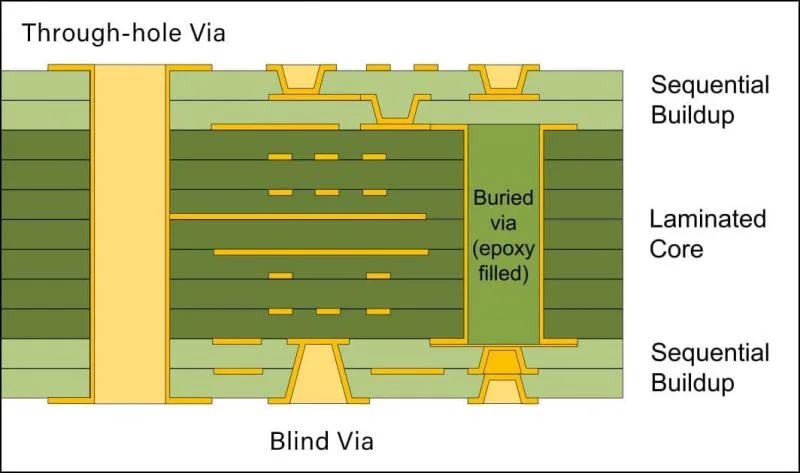
What Are Blind Vias and Why Do They Matter
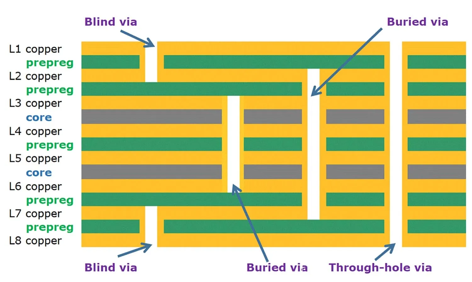
Blind vias are specialized interconnections in multilayer PCBs that connect an outer layer to one or more inner layers without penetrating the entire board. Unlike through hole vias, they remain invisible from the opposite side, saving space and enabling denser layouts. Their importance in modern PCB design cannot be overstated, especially in high density interconnect boards where component spacing is tight. Blind vias reduce signal path lengths, minimize parasitic effects, and support finer pitch components. However, their placement directly impacts signal integrity, influencing factors like signal delay, noise, and electromagnetic interference. Poorly positioned blind vias can disrupt impedance continuity and degrade performance in high speed circuits. For engineers, mastering their use is essential to meet the demands of advanced electronics.
Related Reading: Unlocking PCB Density: A Beginner's Guide to Blind Vias
Technical Principles of Blind Vias and Signal Integrity
Signal integrity refers to the preservation of an electrical signal’s quality as it travels through a PCB. It is affected by factors such as impedance, crosstalk, and signal reflection. Blind vias, while beneficial for space optimization, introduce discontinuities in the signal path if not carefully designed. When a high speed signal transitions through a blind via from one layer to another, any mismatch in impedance can cause reflections, leading to data errors. Additionally, the stub effect, where an unused portion of a via acts as a resonant structure, can degrade signal quality. The proximity of blind vias to other traces or vias can also induce crosstalk, especially in densely populated designs. Understanding these mechanisms is vital for engineers aiming to maintain clean signal transmission.
The aspect ratio of blind vias, defined as the ratio of depth to diameter, plays a significant role in their performance. A high aspect ratio can complicate manufacturing and affect reliability, potentially leading to signal loss. Standards such as IPC-6012E provide guidelines on acceptable aspect ratios for vias to ensure manufacturability and performance. Furthermore, the dielectric material surrounding the via influences signal propagation speed and loss. Engineers must account for these material properties during the design phase to predict and mitigate potential issues related to signal integrity.
Placement Strategies for Optimal Signal Integrity
Strategic placement of PCB blind vias is crucial to minimize their negative impact on signal integrity. Below are key strategies tailored for electrical engineers working on high speed and high density designs.
Minimize Via Stubs
Via stubs occur when a blind via extends beyond the connected layers, leaving an unterminated section. This stub can resonate at specific frequencies, causing signal distortion. To avoid this, designers should place blind vias such that they connect only the necessary layers without excess depth. Back drilling, a process to remove unused via portions, can also be applied in cases where stubs are unavoidable. Adhering to guidelines in IPC-6012E ensures that via structures meet performance specifications.
Optimize Via to Trace Proximity
Placing blind vias too close to high speed traces can induce crosstalk due to electromagnetic coupling. Maintaining adequate spacing between vias and sensitive traces reduces this risk. A general rule is to keep vias at least three times the via diameter away from critical signal lines. This spacing helps in managing field interactions and preserving signal integrity. Simulation tools can aid in determining precise distances based on specific design parameters.
Control Impedance with Reference Planes
Blind vias should be placed near reference planes, such as ground or power planes, to maintain consistent impedance. A nearby reference plane provides a return path for signals, reducing loop inductance. When routing differential pairs, ensure that blind vias for both traces are symmetrically placed relative to the reference plane. This symmetry minimizes skew and maintains signal timing. Guidelines from IPC-A-600K can be referenced for acceptable board layer configurations.
Avoid Clustering in High Density Areas
Clustering multiple blind vias in a small area can lead to manufacturing challenges and signal interference. Distribute vias evenly across the design to prevent localized stress and thermal issues during fabrication. Even distribution also helps in managing signal paths and reducing potential crosstalk. For high density interconnect designs, staggering via placements can further optimize space without compromising integrity.
Use Ground Vias for Shielding
Placing ground vias near signal blind vias can act as a shield, reducing electromagnetic interference. These ground vias provide a low impedance return path and help contain stray fields. This strategy is particularly effective in high speed designs where noise suppression is critical. Positioning ground vias strategically around sensitive signal vias enhances overall board performance.
Practical Applications in High Speed Designs
In high speed PCB designs, such as those for telecommunications or data centers, blind vias are often used under fine pitch components like ball grid arrays. Their placement directly affects signal timing and data rates. For instance, in a design operating at multi gigabit speeds, placing blind vias to minimize path length differences in differential pairs ensures timing alignment. Engineers can use simulation software to model via effects before fabrication, identifying potential issues in signal integrity. Following standards like IPC-6012E during the design phase guarantees that the vias meet both performance and manufacturing criteria.
Another application is in multilayer boards where blind vias connect outer layers to internal signal layers, avoiding interference with other components. Careful placement ensures that these vias do not disrupt power distribution networks. By integrating the strategies mentioned earlier, engineers can achieve reliable performance even in complex layouts. Continuous reference to industry standards ensures consistency and quality in the final product.
Related Reading: Blind Vias in PCB Design: Optimizing High-Density Boards
Troubleshooting Common Issues with Blind Via Placement
Even with careful planning, issues related to blind via placement can arise during PCB design or testing. One common problem is unexpected signal reflection due to impedance mismatches at via transitions. Engineers can address this by reviewing the stackup design and ensuring that blind vias are aligned with reference planes as per IPC-A-600K guidelines. If reflections persist, adjusting the via pad size or anti pad dimensions might help in fine tuning impedance.
Another frequent issue is crosstalk between adjacent blind vias in dense designs. Increasing the spacing or adding ground vias as shields can mitigate this problem. During testing, if noise levels are higher than expected, engineers should inspect via to via distances and compare them against design rules. Iterative adjustments based on test results can refine placement for optimal signal integrity.
Conclusion
Achieving optimal signal integrity in PCB design requires meticulous attention to the placement of blind vias. These structures, while essential for high density and high speed applications, can introduce challenges if not strategically positioned. By minimizing via stubs, optimizing proximity to traces, controlling impedance with reference planes, avoiding clustering, and using ground vias for shielding, engineers can significantly enhance performance. Adhering to established industry standards ensures that designs are both manufacturable and reliable. As electronic systems continue to evolve, mastering blind via placement strategies will remain a critical skill for electrical engineers aiming to push the boundaries of innovation.
FAQs
Q1: How do PCB blind vias affect signal integrity in high speed designs?
A1: Blind vias can impact signal integrity by introducing impedance discontinuities and potential crosstalk in high speed designs. If not placed correctly, they may cause signal reflections or delays. Strategically positioning them near reference planes and maintaining proper spacing minimizes these effects. Following industry guidelines ensures that signal quality remains intact even at high frequencies.
Q2: What are the best placement strategies for PCB blind vias?
A2: Effective placement strategies for PCB blind vias include minimizing stubs, maintaining spacing from critical traces, and aligning with reference planes. Distributing vias evenly prevents manufacturing issues, while ground vias can shield against interference. These approaches help preserve signal integrity and ensure reliable performance in complex layouts.
Q3: Why is signal integrity crucial when using blind vias in multilayer PCBs?
A3: Signal integrity is vital in multilayer PCBs with blind vias because any degradation can lead to data errors or system failures. Blind vias, if poorly placed, can disrupt signal paths and cause noise. Ensuring their strategic placement maintains clean transmission, which is essential for the functionality of modern electronic devices.
Q4: How can engineers test the impact of blind via placement on signal integrity?
A4: Engineers can test blind via placement impact on signal integrity using simulation tools during design and oscilloscopes during prototyping. Time domain reflectometry can identify impedance mismatches, while eye diagrams assess signal quality. Iterative testing and adjustments based on results help optimize via positioning for minimal signal distortion.
References
IPC-6012E — Qualification and Performance Specification for Rigid Printed Boards. IPC, 2020.
IPC-A-600K — Acceptability of Printed Boards. IPC, 2020.