Introduction
As an electronic hobbyist, diving into advanced printed circuit board (PCB) design opens up exciting possibilities for compact and efficient projects. One key concept to explore is blind vias, a technique often used in high-density designs. Blind vias for hobbyists might seem intimidating at first, but with a simple explanation, they become accessible even for beginners. This guide will break down what blind vias are, why they matter, and how to incorporate them into your DIY PCB projects. Whether you are crafting a small gadget or experimenting with multilayer boards, understanding this technology can elevate your skills. Written with a logical and structured approach, this article aims to provide an easy blind via explanation and serve as a beginner's guide to blind vias, helping you navigate the complexities of simple PCB design with blind vias.
What Are Blind Vias and Why Do They Matter
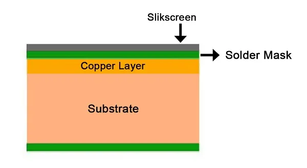
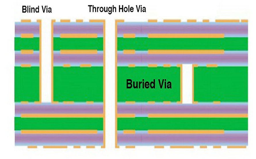
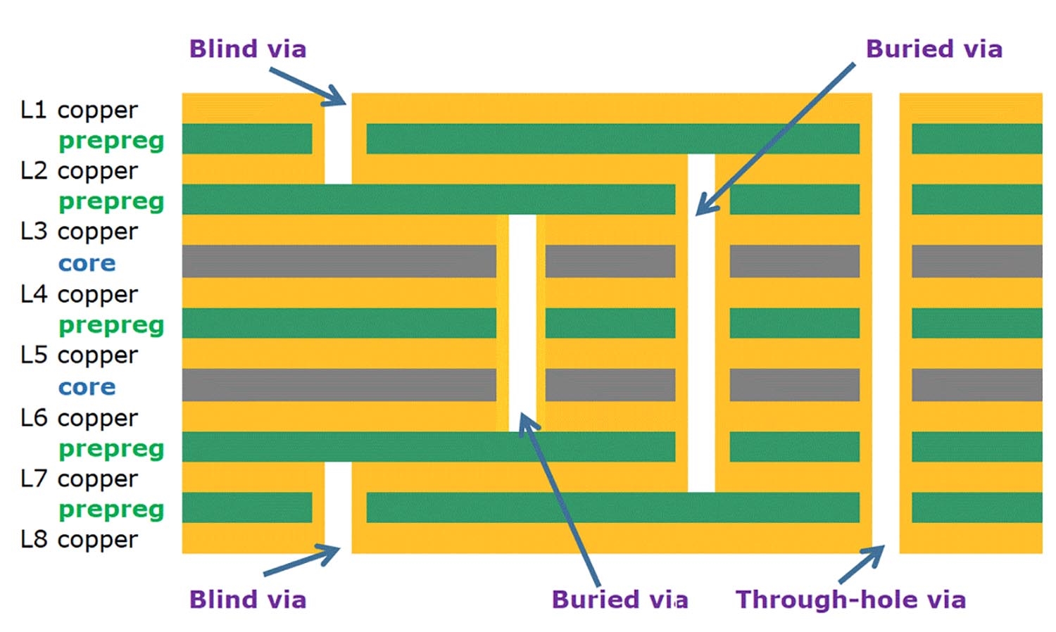
Blind vias are a type of connection in multilayer PCBs that link an outer layer to an inner layer without passing through the entire board. Unlike traditional through-hole vias that span from top to bottom, blind vias are only visible on one side of the board, hence the term "blind." This unique structure allows for more efficient use of space, making them essential for high-density interconnect (HDI) designs often found in compact electronics.
For hobbyists, the importance of blind vias lies in their ability to save space and improve design flexibility. When working on small projects like wearable devices or miniature sensors, every millimeter counts. Blind vias enable tighter component placement and better signal routing by freeing up space on the opposite side of the board. They also help reduce signal interference in high-speed circuits, a common challenge in advanced hobbyist projects. By mastering simple PCB design with blind vias, you can push the boundaries of what your DIY creations can achieve.
Related Reading: Unlocking PCB Density: A Beginner's Guide to Blind Vias
Technical Principles of Blind Vias
Understanding how blind vias work requires a basic grasp of PCB layer structure. A multilayer PCB consists of several conductive copper layers separated by insulating material. Vias serve as electrical connections between these layers. In the case of blind vias, they are drilled or laser-etched from one surface to a specific inner layer, stopping before reaching the opposite side. This partial connection is typically achieved using advanced manufacturing techniques like sequential lamination or laser drilling, which ensure precision.
The primary advantage of this design is space optimization. Since blind vias do not penetrate the entire board, the opposite side remains available for other traces or components. Additionally, they can improve signal integrity by shortening connection paths, which is crucial for high-frequency signals often encountered in modern hobbyist projects like radio frequency modules. However, their complexity means that not all standard manufacturing processes support them, and hobbyists must plan carefully when incorporating blind vias into designs.
Another key principle is their role in thermal management. Blind vias can help dissipate heat from components on the surface layer to an inner ground plane, though they are less effective than through-hole vias for this purpose. According to standards like IPC-6012E, which governs the performance of rigid printed boards, the design and placement of such vias must meet strict criteria to ensure reliability. For hobbyists, adhering to these principles ensures that your PCB withstands operational stresses.
Practical Tips for Using Blind Vias in Hobbyist Projects
Incorporating blind vias into your PCB designs as a hobbyist requires careful planning, especially since they are more complex than standard vias. Below are actionable steps to help you integrate blind vias for hobbyists into your projects while maintaining simplicity and effectiveness.
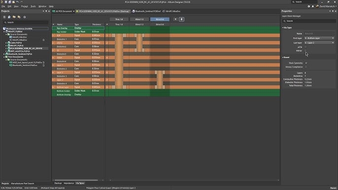
- Start with design software that supports multilayer configurations. Ensure that the tool allows you to define blind vias explicitly in the layer stackup. This step is critical for generating accurate manufacturing files.
- Keep the design simple by limiting the number of layers. For beginners, a four-layer board with blind vias connecting the top layer to the first inner layer is a manageable starting point.
- Pay attention to aspect ratio, which is the ratio of via depth to diameter. Standards like IPC-6012E recommend maintaining a balanced aspect ratio to avoid manufacturing issues. As a hobbyist, aim for larger via diameters if possible to simplify fabrication.
- Consult with your chosen fabrication service early in the design process. Many low-cost manufacturers may not support blind vias or may impose additional constraints. Clarify their capabilities before finalizing your layout.
- Test your design with a prototype. Since blind vias add complexity, producing a small batch first helps identify potential issues like poor connections or misalignment without significant cost.
While blind vias offer space-saving benefits, they can increase manufacturing expenses. For hobbyists on a budget, consider if the design truly requires them or if alternative routing methods can achieve similar results. Balancing functionality with cost is key to practical simple PCB design with blind vias.
Related Reading: Blind Vias in PCB Design: Optimizing High-Density Boards
Common Challenges and Solutions for Beginners
As a beginner exploring blind vias, you might encounter several hurdles. One frequent issue is the difficulty in visualizing connections in a multilayer board. Without seeing through the entire PCB, ensuring correct routing can be tricky. To overcome this, rely on 3D view features in design software to inspect layer interactions. This visual aid can prevent mistakes before manufacturing begins.
Another challenge is the risk of signal integrity problems, especially in high-speed designs. Blind vias can introduce impedance discontinuities if not designed properly. A practical solution is to keep signal paths as short as possible and place ground planes near critical signals to minimize interference. Referencing guidelines from IPC-A-600K on acceptability of printed boards can help ensure your design meets quality expectations.
Finally, manufacturing limitations often pose a barrier for hobbyists. Not all affordable fabrication services offer blind via capabilities, and those that do may require specific design rules. Always review the manufacturer’s design guidelines and adjust your layout accordingly. Starting with a beginner's guide to blind vias like this one can help you avoid common pitfalls and build confidence in using advanced techniques.
Benefits of Blind Vias for Hobbyist Projects
For electronic hobbyists, adopting blind vias brings several advantages that can transform your projects. First, they allow for greater component density. When space is limited, such as in a custom smartwatch or a miniature drone controller, blind vias free up room for additional features or smaller form factors. This capability aligns with the trend of increasingly compact electronics.
Second, blind vias can enhance the aesthetic and functional quality of your PCB. By reducing visible holes on one side, they create a cleaner look, which is appealing for exposed boards in display projects. Functionally, they support better organization of complex circuits by separating high-speed and low-speed signals across layers.
Lastly, learning to use blind vias equips you with skills applicable to professional-grade designs. As you progress from hobbyist to advanced designer, familiarity with HDI techniques positions you to tackle sophisticated projects. An easy blind via explanation like the one provided here can be your stepping stone to mastering these concepts.
Conclusion
Blind vias represent a powerful tool for electronic hobbyists eager to advance their PCB design skills. By understanding their purpose, technical principles, and practical applications, you can create more compact and efficient projects. This beginner's guide to blind vias has covered the essentials, from their space-saving benefits to the challenges of implementation. With careful planning and adherence to industry standards like IPC-6012E and IPC-A-600K, even beginners can achieve success with simple PCB design using blind vias. As you experiment and prototype, the knowledge of blind vias for hobbyists will open new doors for innovation in your DIY electronics journey.
FAQs
Q1: What are blind vias, and why should hobbyists care about them?
A1: Blind vias connect an outer PCB layer to an inner layer without passing through the entire board. For hobbyists, they are valuable in simple PCB design with blind vias because they save space, allowing for denser component placement in compact projects like wearables. They also improve signal routing, making them a stepping stone to advanced designs.
Q2: How can I start using blind vias as a beginner in PCB design?
A2: Begin with design software supporting multilayer boards and blind via definitions. Start with a basic four-layer design, focusing on a beginner's guide to blind vias for guidance. Check with your fabrication service for their capabilities and design rules. Prototyping helps identify issues early in the learning process.
Q3: Are blind vias expensive for hobbyist projects?
A3: Yes, blind vias for hobbyists often increase manufacturing costs compared to standard through-hole vias due to their complexity. However, the cost varies based on the fabrication service and board specifications. Balance the need for space savings against budget constraints before opting for blind vias in your design.
Q4: What challenges might I face with blind vias in simple PCB design?
A4: In simple PCB design with blind vias, hobbyists may struggle with visualizing multilayer connections and ensuring signal integrity. Use 3D views in design tools to check routing. Manufacturing limitations can also be an issue, so always review fabricator guidelines to avoid design errors.
References
IPC-6012E — Qualification and Performance Specification for Rigid Printed Boards. IPC, 2020.
IPC-A-600K — Acceptability of Printed Boards. IPC, 2020.