Introduction
Ceramic PCBs serve critical roles in high-power electronics, RF applications, and environments demanding superior thermal management. Their unique material properties, such as exceptional thermal conductivity and low coefficient of thermal expansion, make them ideal for demanding conditions where standard organic substrates fail. However, assembling components on ceramic PCBs introduces specific challenges due to their brittleness and heat dissipation characteristics. Ceramic PCB soldering requires precise control to prevent cracks or delamination, while component placement demands accuracy to mitigate stress concentrations. Mastering these processes ensures reliable performance and longevity in applications like power converters and aerospace systems. This article outlines practical best practices tailored for electric engineers handling SMT assembly ceramic PCB workflows.
Understanding Ceramic PCBs and Assembly Challenges
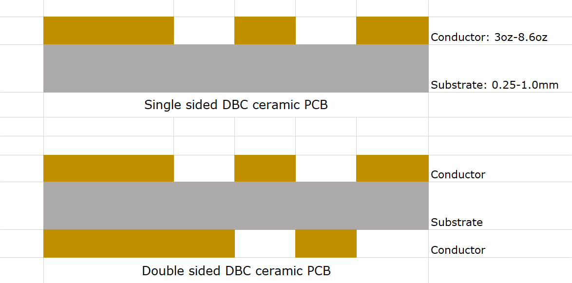
Ceramic PCBs, typically made from alumina, aluminum nitride, or similar substrates, offer thermal conductivities far exceeding those of FR4 boards. This high heat spreading capability affects soldering by rapidly dissipating applied energy, necessitating adjusted process parameters for uniform reflow. Brittleness poses risks during handling and placement, where mechanical stress can propagate micro-cracks invisible to the naked eye. Coefficient of thermal expansion mismatches between the ceramic substrate and attached components further complicate ceramic PCB soldering, potentially leading to solder joint fatigue over thermal cycles. Engineers must prioritize substrate preparation, including thorough cleaning to remove particulates that could cause voids. Adhering to these principles aligns assembly with industry expectations for robustness.
Component placement guidelines become crucial here, as improper positioning amplifies stress points around pads. High component density on ceramic PCBs exacerbates heat management issues during reflow soldering ceramic PCB processes. Wave soldering ceramic PCB, though less common, introduces flux entrapment risks due to the substrate's non-porous surface. Overall, these factors demand a troubleshooting-focused approach to achieve high yields.
Material Properties Influencing Assembly
The core appeal of ceramic substrates lies in their thermal properties, enabling efficient heat dissipation in compact designs. Low CTE values minimize warpage compared to organic laminates, but rapid cooling post-soldering can still induce tensile stresses. Metallization layers, often direct bonded copper or thick-film prints, must withstand soldering temperatures without peeling. Solder paste interaction with these metal finishes requires compatible alloys to ensure wetting without excessive intermetallic growth. Engineers should evaluate substrate thickness and copper weight early, as thicker ceramics demand longer preheat times for even heating.
Handling during transit adds another layer, with fixtures recommended to prevent edge chipping. These properties directly impact SMT assembly ceramic PCB outcomes, where precision pick-and-place machines benefit from fiducial marks optimized for vision systems.
Component Placement Guidelines for Ceramic PCBs
Effective component placement starts with land pattern design following IPC-7351 guidelines for surface mount footprints. Larger toe and heel fillets accommodate the high thermal mass of ceramic substrates, promoting better solder flow. Place heat-generating components centrally or near heat sinks to leverage the board's conductivity, avoiding thermal shadows that cause uneven reflow. Maintain minimum spacing between parts to allow stencil release and prevent bridging, typically scaling with fine-pitch requirements.
Fiducials should be asymmetrically placed for accurate machine alignment, compensating for any substrate tolerances. Orient components to minimize shear stress from CTE differences, such as aligning leads parallel to potential flex directions. For mixed through-hole and SMT, position thru-hole parts first to stabilize the board during reflow. These component placement guidelines reduce defects like tombstoning, common in high-conductivity environments.
Support pallets cradle the board undersides, preventing sagging under conveyor heat. Validate placements with automated optical inspection post-pick-and-place to catch offsets early.
Preparation Steps Before Soldering
Surface preparation forms the foundation of successful ceramic PCB soldering. Ultrasonic or plasma cleaning removes oxides and residues from metallized pads without damaging the brittle base. Apply solder paste via laser-cut stencils with apertures tuned for 100-125% paste volume relative to pad area, ensuring release on non-wetting ceramics. Verify paste thickness uniformity with SPI to avoid insufficient bridges or excess slumping.
Stencil alignment tolerances tighten to under 25 microns for fine-pitch devices. Bake boards if moisture-sensitive, classifying per J-STD-020 to prevent popcorning during ramp-up. These steps set the stage for reliable SMT assembly ceramic PCB.
Best Practices for Reflow Soldering Ceramic PCBs
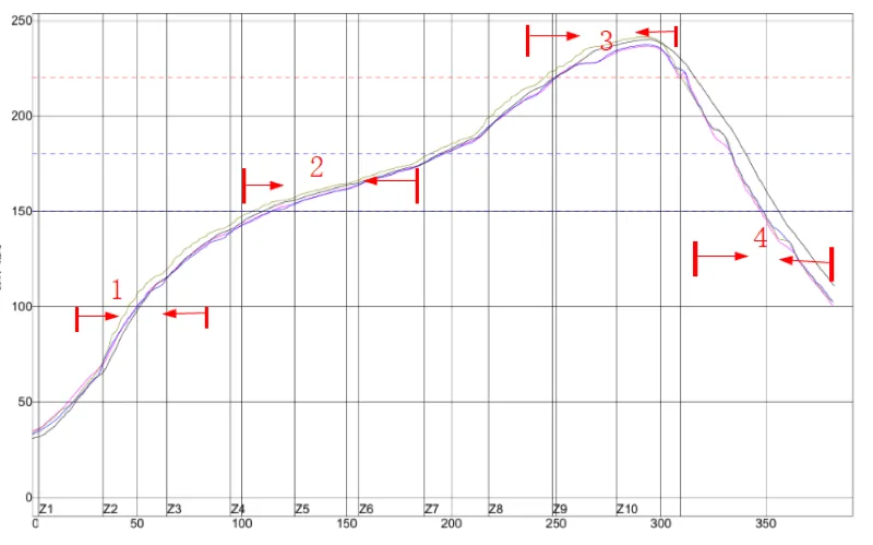
Reflow soldering ceramic PCB stands as the preferred method for surface mount assemblies due to its controlled atmosphere and profile flexibility. Develop custom profiles with gradual ramp rates to match the substrate's high thermal diffusivity, ensuring all joints reach liquidus simultaneously. Nitrogen purging minimizes oxidation on copper traces, enhancing joint integrity. Peak temperatures and times above liquidus follow component datasheets, with soak phases allowing flux activation.
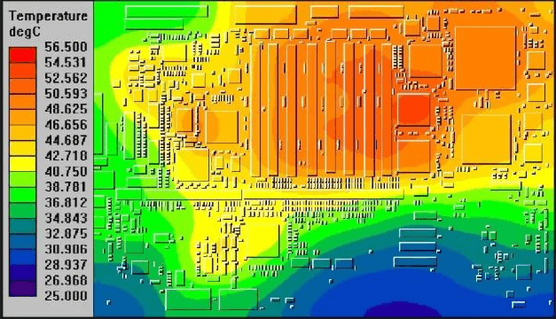
Monitor profiles using thermocouples attached to test coupons mimicking production boards. Convection ovens provide the most uniform heating for ceramics, outperforming IR in edge-to-edge consistency. Post-reflow cooling occurs in stages to relieve stresses gradually.
IPC-A-610 criteria guide visual and X-ray inspections for fillet formation and voiding. This approach yields robust joints resilient to vibration.
Wave Soldering Ceramic PCB: Considerations and Techniques
Wave soldering ceramic PCB suits through-hole or selective mixed assemblies, but demands flux chemistry compatible with non-absorbent surfaces. Preheat zones compensate for rapid heat sink-away, targeting flux activation without charring. Single or dual-wave pallets mask SMT areas, supporting the board to avoid immersion-induced cracks.
Flux drag-out poses cleaning challenges, requiring deionized water rinses followed by drying. Limit dwell times to prevent copper dissolution. While less ideal than reflow for full SMT, wave excels in high-volume thru-hole scenarios when profiles align with J-STD-020 limits.
Troubleshoot bridging by optimizing wave height and conveyor speed.
Inspection and Quality Assurance
Post-assembly inspection verifies solder joint acceptability per IPC-A-610, focusing on wetting, voids, and head-in-pillow defects prevalent on ceramics. AOI detects bridges and misalignments, while X-ray reveals subsurface issues like delamination. Cross-section analysis on samples confirms intermetallic thickness.
Shear and pull tests quantify mechanical strength, correlating to thermal cycle reliability. Traceability logs process parameters for root-cause analysis.
Troubleshooting Common Assembly Issues
Cracking often stems from thermal shock; mitigate with profiled preheats and handling jigs. Voids arise from paste starvation or outgassing, addressed by optimized stencil volumes and nitrogen reflow. Tombstoning links to uneven heating, resolved by symmetric pad designs per IPC-7351.
Delamination signals poor metallization adhesion, preventable via qualified suppliers. Solder balls result from stencil wear, fixed by routine maintenance. Systematic data collection pinpoints trends for process tweaks.
Conclusion
Ceramic PCB assembly thrives on meticulous soldering and placement practices tailored to material uniqueness. Reflow soldering ceramic PCB offers precision for SMT, while wave soldering ceramic PCB fits selective needs. Component placement guidelines and standards like IPC-7351 ensure stress minimization. Implementing these yields high-reliability boards for demanding applications. Engineers gain troubleshooting edge through profile validation and inspections. Prioritize these for optimal outcomes.
FAQs
Q1: What are the key differences in reflow soldering ceramic PCB compared to FR4?
A1: Reflow soldering ceramic PCB requires slower ramp rates due to high thermal conductivity, preventing uneven heating. Profiles must account for rapid dissipation, often needing extended soaks for flux action. Nitrogen atmospheres prove essential to curb oxidation on metallized surfaces. Follow J-STD-020 for classification to avoid thermal shock. This ensures uniform joints without cracks.
Q2: How do component placement guidelines impact ceramic PCB soldering reliability?
A2: Component placement guidelines emphasize IPC-7351 land patterns to balance solder volume and stress distribution. Central heat source positioning leverages conductivity for even reflow. Adequate spacing prevents bridging during SMT assembly ceramic PCB. Fiducials enhance pick-and-place accuracy. Poor adherence leads to tombstoning or fatigue failures.
Q3: Is wave soldering ceramic PCB recommended for high-density SMT?
A3: Wave soldering ceramic PCB suits thru-hole better than dense SMT due to flux and immersion risks. Masking protects placed components, but preheat uniformity challenges persist. Reflow generally outperforms for density. Use when volume justifies pallets. Inspect rigorously for entrapment per IPC-A-610.
Q4: What troubleshooting steps address cracks in ceramic PCB soldering?
A4: Examine thermal profiles for shock indicators like steep ramps. Verify handling avoids flexure on brittle substrates. Cross-section cracks to assess origins, such as CTE mismatch. Adjust preheats and use support fixtures. Qualify pastes for compatibility. Repeat tests post-correction.
References
IPC-7351B — Generic Requirements for Surface Mount Design and Land Pattern Standard. IPC, 2010
IPC-A-610G — Acceptability of Electronic Assemblies. IPC, 2017
J-STD-020E — Moisture/Reflow Sensitivity Classification for Nonhermetic Surface Mount Devices. JEDEC, 2014


