Why is PCB layer thickness a critical design decision?
The thickness of a printed circuit board, both overall and for its individual layers, significantly influences its performance characteristics, mechanical robustness, and manufacturability. This fundamental design choice can determine a project's success or failure. While a standard PCB thickness of 1.6 mm (0.063 inches) is a common starting point, it's not universally applicable. Designers must consider various factors, including the intended application, desired electrical properties, and potential mechanical stresses the board will endure.
Making an informed decision about layer thickness goes beyond merely selecting a dimension. It involves a deep understanding of how different thicknesses impact everything from signal integrity in high-frequency circuits to the board's ability to dissipate heat. Therefore, a thorough evaluation of these parameters is essential for crafting a reliable and efficient PCB.
How does layer thickness impact PCB functionality?
The physical dimensions of a PCB's layers directly affect several key operational aspects. Electrically, layer thickness plays a vital role in impedance control; thinner dielectric layers, for instance, can help achieve lower impedance, while thicker ones are often necessary for high-voltage applications to prevent electrical breakdown. Mechanically, a thicker board inherently offers greater durability, making it more suitable for environments subject to vibrations or physical impact, such as in automotive or industrial settings.
Furthermore, thermal management is heavily influenced by copper layer thickness. Thicker copper planes and traces can conduct more current without excessive temperature rise, thereby enhancing the board's reliability and lifespan. Finally, the choice of thickness has practical implications for cost and production. Deviating from standard thicknesses can lead to higher manufacturing expenses and extended lead times, as it might necessitate custom materials or adjustments to the fabrication process.
What are common PCB thickness standards?
When beginning a new PCB project, understanding the widely accepted thickness standards is a crucial first step. These standards provide a baseline that often balances cost-effectiveness with practical design requirements, making the manufacturing process smoother and more predictable.
Exploring standard PCB dimensions
The most prevalent thickness for PCBs across the industry is 1.6 mm (approximately 0.063 inches). This dimension has become a de facto standard due to its optimal balance of mechanical strength, material availability, cost efficiency, and compatibility with a broad range of electronic components and assembly hardware. However, it's important to recognize that this is not the only option. Other commonly utilized thicknesses include 0.8 mm, 1.0 mm, and 2.0 mm, with even thicker boards (up to 3.2 mm) reserved for specialized applications demanding exceptional rigidity or current-carrying capacity.
Choosing a standard thickness is often advantageous because it aligns with readily available raw materials and established manufacturing processes, which can minimize production costs and lead times. Opting for a non-standard thickness, such as 1.2 mm, while technically feasible, might incur additional expenses or delays due to the need for custom material procurement or adjustments to the fabrication line. Therefore, unless specific design constraints dictate otherwise, beginning with a standard thickness like 1.6 mm is typically a prudent choice.
What factors dictate optimal PCB layer thickness?
Selecting the ideal layer thickness for a PCB is a multifaceted decision influenced by various technical and environmental considerations. A thorough understanding of these factors ensures that the final design meets both performance objectives and practical manufacturing constraints.
Key elements guiding thickness choices
The intended application and the operational environment are primary determinants. For example, compact consumer devices like smartphones often use ultra-thin boards (0.8 mm or less) to conserve space, whereas industrial control systems or automotive electronics typically demand thicker boards (2.0 mm or more) to withstand severe vibrations, extreme temperatures, and other harsh conditions.
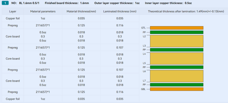
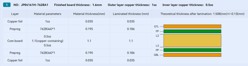
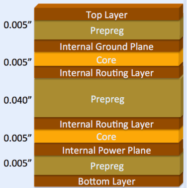
The overall PCB layer stackup and the total number of layers also play a significant role. A simple 2-layer board might be as thin as 0.8 mm, while a complex 6- or 8-layer design could easily reach 1.6 mm or more, primarily due to the inclusion of multiple copper and dielectric layers. Within the stackup, the dielectric thickness between layers is critical for signal integrity, especially in high-speed applications where precise impedance control (e.g., 50 ohms for RF signals) necessitates very thin dielectric layers, sometimes as fine as 0.1 mm.
Impact of current, signals, and manufacturing on thickness
The current-carrying capacity required by the circuit directly relates to the copper layer thickness, often measured in ounces per square foot (oz/ft²). A standard 1 oz copper layer (approximately 0.035 mm thick) can handle a certain current level, but high-power applications might require 2 oz (0.07 mm) or even 3 oz copper, which contributes to the overall board thickness and aids in thermal dissipation.
For high-frequency or high-speed digital designs, precise layer thickness is paramount for maintaining signal integrity. The dielectric thickness between a signal trace and its reference plane (ground or power) directly influences the characteristic impedance. Adjusting these thicknesses is often necessary to achieve desired impedance values.
Finally, manufacturing tolerances are an unavoidable consideration. PCB thickness tolerance refers to the acceptable variation in the final board thickness, typically around ±10% for standard boards. Tighter tolerances are achievable but usually come with increased costs, requiring designers to assess if their application can accommodate standard variations or if a stricter, more expensive tolerance is justified.
How can a PCB thickness calculator assist designers?
Accurately determining the appropriate layer thickness for a PCB can be a complex task, especially for multilayer designs where numerous variables interact. Fortunately, a multilayer PCB thickness calculator serves as an invaluable tool to simplify this process, providing precise estimations based on specified design parameters.
Leveraging digital tools for stackup design
A PCB thickness calculator streamlines the intricate process of creating an effective PCB layer stackup. To use it efficiently, designers typically input several key pieces of information. This includes specifying the total number of layers (e.g., 2-layer, 4-layer, 6-layer), as each additional layer contributes to the overall board dimension. Next, details about the core and prepreg materials, such as FR-4, are entered, along with their individual dielectric thicknesses. For instance, a common prepreg might be 0.2 mm thick.
The calculator also requires the copper weight (e.g., 1 oz or 2 oz) for each layer, which influences both the electrical characteristics and the total thickness. Once all parameters are entered, the tool computes an estimated total board thickness. This calculation helps designers verify if the proposed stackup meets their target dimensions and ensures that the board satisfies both electrical and mechanical specifications without extensive trial-and-error, thereby saving significant design time and resources.
What materials are commonly used for PCB layers?
The selection of materials is fundamental to defining PCB layer thickness and overall performance. The properties of these materials directly impact the board's electrical characteristics, mechanical strength, and thermal management capabilities.
Common PCB substrate and dielectric materials
The most ubiquitous substrate material is FR-4, an abbreviation for Flame Retardant level 4. This fiberglass-reinforced epoxy laminate is widely favored due to its balanced properties, including a dielectric constant of approximately 4.5 and a thermal conductivity of around 0.25 W/m·K. FR-4 is available in various standard thicknesses for both core and prepreg (bonding) layers, typically ranging from 0.1 mm to 0.5 mm, which are then combined to achieve the desired total board thickness.
For applications requiring different performance characteristics, alternative materials are employed. High-frequency laminates, such as Rogers or Teflon, feature lower dielectric constants (e.g., 2.2-3.0), making them ideal for RF and microwave circuits where signal speed and minimal loss are critical. These materials are often used in thinner constructions. Flexible PCBs commonly utilize polyimide substrates, which are remarkably thin (typically 0.05 mm to 0.1 mm) to provide necessary flexibility, though they offer less mechanical rigidity than FR-4. For high-power applications requiring superior heat dissipation, metal-core PCBs are a solution, often incorporating thicker substrates (1.0 mm or more) with a metallic base to efficiently draw heat away from components.
Essential tips for designing an effective PCB layer stackup
A meticulously planned PCB layer stackup is crucial for achieving optimal electrical performance, managing thermal loads, and ensuring the mechanical integrity of the final product. Implementing specific design strategies can significantly enhance the reliability and manufacturability of your circuit board.
Best practices for stackup design
Aim for a symmetrical layer arrangement to minimize the risk of warping during the manufacturing process, which can occur due to uneven thermal expansion. For instance, in a 4-layer board, positioning two signal layers on the outer surfaces and two inner layers (dedicated to ground and power planes) centrally creates a balanced structure. To effectively reduce crosstalk and interference, particularly in high-speed designs, ensure adequate dielectric thickness separates signal layers. This helps maintain signal integrity and prevents unwanted coupling.
Prioritize the placement of ground planes as close as possible to signal layers. This configuration provides a low-impedance return path for signals, which is vital for minimizing electromagnetic interference (EMI) and improving signal quality. Achieving this often involves using thinner dielectric layers (e.g., 0.1-0.2 mm) between signal and ground planes. Always communicate with your PCB manufacturer early in the design phase to understand their specific capabilities regarding minimum and maximum layer thicknesses, as well as achievable tolerances. Aligning your design with their processes can prevent costly revisions and production delays.
Common mistakes to avoid when choosing PCB thickness
Even seasoned PCB designers can fall prey to specific errors when determining layer thickness, leading to performance issues or manufacturing challenges. Awareness of these common pitfalls can save significant time and resources.
Pitfalls to bypass in thickness selection
A frequent misstep is defaulting to a standard 1.6 mm thickness without thoroughly assessing whether the application truly demands a thinner or thicker board. This oversight can result in suboptimal electrical performance or insufficient mechanical robustness. Another common error is neglecting to account for PCB thickness tolerance. Manufacturing variations mean the final board thickness might deviate slightly from the specified value; failing to design for this acceptable range can lead to incompatibility with enclosures or connectors.
Underestimating the thermal impact of high-current traces on thin copper layers is a critical mistake that can lead to localized overheating and reduced component reliability. Always ensure that copper thickness is sufficient for the expected current load. Lastly, opting for a non-standard or custom thickness without a clear and justifiable technical reason is often an unnecessary expense. Such choices can significantly increase manufacturing costs and extend production timelines, so custom thicknesses should only be specified when absolutely essential for performance.


