Introduction
Plated Through-Holes (PTHs) are fundamental to the structural and electrical integrity of most multilayer printed circuit boards. They serve as critical electrical connections between layers and provide mechanical support for component leads. The choice of PTH plating materials is not merely an aesthetic decision; it profoundly impacts the PCB's performance, reliability, manufacturability, and cost. As a manufacturing specialist, I emphasize that understanding these material properties and their implications is crucial for accurate PCB specification and successful production.
What is PTH Plating and Why Material Choice Matters
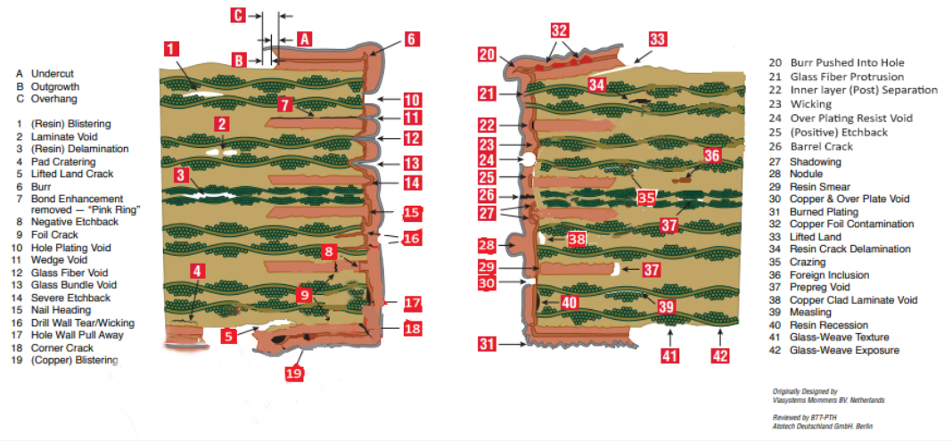
PTH plating is the process of depositing a conductive metal layer onto the walls of drilled holes in a PCB, connecting the conductive patterns on different layers. This process creates the necessary electrical continuity and strengthens the mechanical structure of the through-hole. Initially, a thin layer of electroless copper is deposited, followed by a thicker layer of electrolytic copper. Subsequent plating, often called the "surface finish" or "final finish," is then applied over the copper and exposed pads.
The selection of PTH plating materials directly influences several key aspects of a PCB:
- Electrical Performance: Affects signal integrity, current carrying capacity, and impedance.
- Solderability: Determines how well components can be soldered to the pads and through-holes.
- Corrosion Resistance: Protects the underlying copper from oxidation and environmental degradation.
- Mechanical Strength: Contributes to the durability of component mounting.
- Cost: Different plating materials vary significantly in price, impacting overall manufacturing costs.
- Process Compatibility: Must be compatible with subsequent assembly processes like soldering or wire bonding.
A thoughtful decision regarding PTH plating materials ensures that the PCB meets its functional requirements throughout its lifespan and can be efficiently manufactured and assembled.
Related Reading: Optimizing Plated Through-Hole Design for High-Speed PCB Performance
Common PTH Plating Materials and Their Properties
Several materials are commonly used for PTH plating, each offering distinct advantages and limitations. The most prevalent are copper, tin, and gold.
Copper Plating
Copper is the primary conductive material used for plating the barrel of the through-hole. After drilling, a thin layer of electroless copper is deposited to make the non-conductive hole walls conductive. This is followed by electrolytic copper plating, which builds up the necessary thickness. Copper provides excellent electrical conductivity and good thermal dissipation. Its ductility allows it to withstand thermal expansion and contraction during manufacturing and operation without cracking. The IPC-6012E standard, "Qualification and Performance Specification for Rigid Printed Boards," specifies minimum copper plating thickness for various product classes, typically ranging from 20 to 25 micrometers (µm) for the barrel. This minimum plating thickness is crucial for ensuring adequate current carrying capacity and reliability.
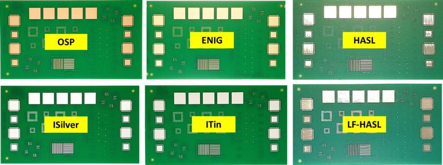
Tin Plating
Tin, often applied as an immersion tin or electrolytic tin, serves primarily as a protective layer over the copper and an excellent solderable surface.
- Hot Air Solder Leveling (HASL): This process applies a eutectic tin-lead or lead-free tin alloy, which is highly solderable. The tin acts as a barrier to copper oxidation, ensuring a long shelf life for solderability.
- Immersion Tin (ImSn): A pure tin layer chemically deposited onto copper. It offers good solderability and a flat surface, making it suitable for fine pitch components. However, whiskers can be a concern with pure tin, which needs mitigation.
- Electrolytic Tin: A thicker, more robust layer of tin, often used where higher wear resistance or specific soldering properties are needed.
Tin plating thickness typically ranges from 1 to 15 µm, depending on the specific tin finish and application. Tin's primary benefits are its low cost and excellent solderability, making it a very common choice for many PCB applications.
Gold Plating
Gold plating is utilized for high-reliability, low-contact resistance, or wire bonding applications. It is significantly more expensive than tin or copper, so its use is typically reserved for specialized PCBs.
- Electroless Nickel Immersion Gold (ENIG): This is a two-layer metallic coating. A layer of electroless nickel is first deposited over the copper, followed by a thin layer of immersion gold. The nickel acts as a barrier layer to prevent copper diffusion into the gold, while the gold provides a highly reliable, corrosion-resistant, and solderable surface with excellent flatness. The gold plating thickness for ENIG is typically very thin, ranging from 0.05 to 0.15 µm.
- Electrolytic Hard Gold: A thicker, harder gold layer applied over a nickel barrier, often used for edge connectors or contact pads that undergo frequent insertion and removal. The gold plating thickness can range from 0.5 to 2.5 µm or more.
Gold offers superior corrosion resistance, excellent electrical contact properties, and is ideal for wire bonding, but its cost limits its use to demanding applications.
Factors Influencing Plating Thickness and Material Choice
The decision regarding PTH plating materials and their corresponding plating thickness is a multi-faceted one, driven by several technical and commercial considerations.
Functional Requirements:
- Current Carrying Capacity: Thicker copper plating is necessary for PTHs carrying higher currents to minimize resistance and heat generation.
- Signal Integrity: For high-speed signals, consistent plating thickness and surface finish flatness are important to maintain impedance control. ENIG is often preferred here due to its flatness.
- Contact Resistance: Applications requiring very low and stable contact resistance, such as edge connectors or button contacts, will opt for gold plating, particularly hard gold.
- Solderability: The ability of solder to wet the surface and form reliable joints is crucial. Tin-based finishes (HASL, Immersion Tin) offer excellent solderability and are cost-effective. ENIG also provides good solderability, but the nickel layer underneath can sometimes lead to issues if the nickel surface is not properly prepared or if soldering cycles are excessive. The J-STD-003C standard, "Solderability Tests for Printed Boards," outlines methods for evaluating PCB solderability.
- Corrosion Resistance: PCBs operating in harsh environments require highly corrosion-resistant finishes. Gold plating excels in this regard due to its inertness. Tin also provides good corrosion protection for the underlying copper.
- Wire Bonding Compatibility: For advanced packaging where bare die are directly attached to the PCB, wire bonding is employed. Gold surfaces are essential for gold wire bonding, and aluminum wire bonding requires specific surface metallurgies. ENIG is a common choice for these applications.
- Cost: Cost is a significant driver. Copper and tin-based finishes are considerably less expensive than gold. The specified plating thickness also directly impacts material consumption and cost. Balancing performance needs with budgetary constraints is a key aspect of PCB specification.
- Shelf Life: The duration for which a PCB can be stored before assembly without compromising solderability is influenced by the finish. Finishes that prevent copper oxidation, such as HASL, Immersion Tin, and ENIG, offer good shelf life.
By carefully evaluating these factors against the product's requirements and applying relevant industry standards like IPC-6012E, manufacturers can make informed decisions about PTH plating materials and their appropriate thickness.
Practical Considerations and Best Practices for Selection
Choosing the right PTH plating materials requires collaboration between design and manufacturing teams. Several practical considerations and best practices can guide this selection process.
- Early Design for Manufacturability (DfM) Involvement: Engaging manufacturing specialists during the design phase ensures that the chosen plating material and plating thickness are compatible with the assembly processes and capabilities. It helps prevent costly redesigns or manufacturing issues later on.
- Understanding Application Environment: The end-use environment of the product is paramount. For consumer electronics with a typical lifespan, tin-based finishes are often sufficient. For critical applications in aerospace, medical devices, or automotive systems, gold finishes might be mandatory due to their superior reliability and environmental robustness.
- Balancing Performance vs. Cost: Always strive for the most cost-effective solution that still meets all performance and reliability requirements. Over-specifying expensive materials like gold when a tin finish would suffice can unnecessarily inflate product cost.
- Adherence to Industry Standards: Always refer to recognized industry standards such as IPC-6012E for minimum plating thickness and quality criteria. These standards provide a benchmark for acceptable quality and performance. For example, the minimum barrel copper plating thickness in a PTH for Class 2 products is 20 µm, while for Class 3 products it is 25 µm.
- Consider Future Assembly Processes: Think about how the PCB will be assembled. If lead-free soldering is required, ensure the chosen finish is compatible. If components will be re-worked frequently, a robust finish might be needed.
- Supplier Capabilities: Verify that the chosen PCB manufacturer has the expertise and equipment to consistently produce the specified plating material and plating thickness to the required quality levels.
By systematically addressing these points, the selection of PTH plating materials becomes a deliberate engineering decision rather than a default choice, leading to optimized PCB designs and reliable products.
Related Reading: Solving Plated Through-Hole Problems: A PCB Troubleshooting Guide

Conclusion
The selection of PTH plating materials is a critical aspect of PCB design and manufacturing, directly influencing a board's electrical performance, solderability, corrosion resistance, and overall reliability. Copper forms the foundational conductive layer within the through-hole, with its plating thickness being vital for current carrying capacity. Surface finishes like tin plating offer excellent solderability and cost-effectiveness for many applications, while gold plating is reserved for high-reliability, low-contact resistance, or wire bonding scenarios. By carefully considering functional requirements, cost implications, and manufacturing processes, and by adhering to established industry standards such as IPC-6012E, engineers can make informed choices about PTH plating materials and their appropriate plating thickness, ultimately leading to robust and high-performing PCB assemblies.
FAQs
Q1: What are the most common PTH plating materials used in PCBs?
A1: The most common PTH plating materials include copper, which forms the conductive barrel of the hole, and surface finishes like tin plating (e.g., HASL, Immersion Tin) for solderability and protection, or gold plating (e.g., ENIG, Electrolytic Hard Gold) for high-reliability contacts and wire bonding applications. Each material serves specific functional purposes.
Q2: Why is copper plating thickness important for PTHs?
A2: Copper plating thickness is critical for PTHs because it directly impacts the current carrying capacity and thermal reliability of the through-hole. Insufficient copper plating thickness can lead to excessive resistance, localized heating, and potential failure, especially for PTHs carrying higher currents, as outlined by standards like IPC-6012E for rigid printed boards.
Q3: When should I choose gold plating over tin plating for PTHs?
A3: Gold plating (such as ENIG or Electrolytic Hard Gold) is typically chosen over tin plating for PTHs and surface pads in applications requiring very low and stable contact resistance, superior corrosion resistance, high wear cycles (like edge connectors), or for fine pitch components and bare die wire bonding applications. Tin plating is generally more cost-effective for standard solderable surfaces.
Q4: How does plating material choice affect PCB assembly processes?
A4: The choice of PTH plating materials significantly affects PCB assembly processes. Materials like tin plating offer excellent solderability for reflow and wave soldering. Gold plating (ENIG) is ideal for wire bonding. The plating material also influences shelf life, reworkability, and compatibility with lead-free soldering requirements, necessitating careful consideration during PCB specification and manufacturing planning.
References
IPC-A-610G — Acceptability of Electronic Assemblies. IPC, 2017.
IPC-6012E — Qualification and Performance Specification for Rigid Printed Boards. IPC, 2017.
IPC-2221B — Generic Standard on Printed Board Design. IPC, 2012.
J-STD-003C — Solderability Tests for Printed Boards. IPC/JEDEC, 2010.
ISO 9001:2015 — Quality Management Systems. ISO, 2015.


