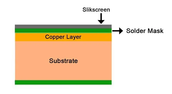
What is PCB Life Cycle Analysis (LCA) and Why is it Essential?
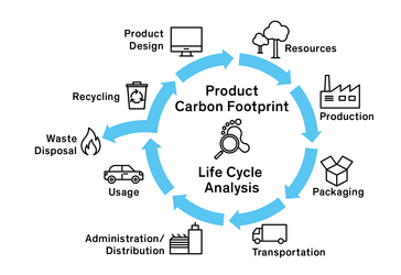
Printed Circuit Board (PCB) Life Cycle Analysis (LCA) is a systematic methodology employed to evaluate the environmental repercussions of a PCB across its entire lifespan. This process, often described as a "cradle-to-grave" examination, encompasses every stage, beginning with the extraction of raw materials, moving through manufacturing, assembly, and active use, and concluding with disposal or recycling. By undertaking a thorough PCB LCA, manufacturers and designers can pinpoint specific areas where energy consumption can be reduced, waste generation minimized, and the overall carbon footprint lowered.
The electronics sector is experiencing exponential growth, with millions of devices being produced annually. PCBs are at the very core of this expansion, yet their production frequently involves hazardous substances, significant energy expenditure, and intricate waste management challenges. A comprehensive PCB environmental impact analysis helps to uncover often-overlooked costs, such as the pollution stemming from chemical etching processes or the emissions generated by energy-intensive production methods. By comprehending these impacts, companies can pivot towards more environmentally sound practices, comply with regulatory demands, and appeal to a growing demographic of environmentally conscious consumers.
Stages of a Complete PCB Life Cycle Analysis
A holistic PCB LCA is structured into several critical stages. Each phase contributes uniquely to the overall environmental footprint, and a detailed understanding of these contributions is fundamental for effective sustainability planning. Let's explore each stage in detail.
Raw Material Sourcing
The journey of a PCB commences with the extraction of its constituent raw materials, which include copper, fiberglass, epoxy resins, and precious metals such as gold and silver. The mining and processing of these materials can lead to considerable environmental degradation, encompassing habitat destruction, widespread water pollution, and high energy consumption. For instance, the production of just one kilogram of copper can result in approximately 3.5 kilograms of CO2 emissions, depending on the specific mining techniques and energy sources employed.
To mitigate environmental impact at this initial stage, it is advisable to prioritize sourcing materials from suppliers who are committed to sustainable mining practices or those who utilize recycled metals. Such choices can significantly reduce the carbon footprint of a PCB even before it enters the manufacturing phase.
Manufacturing and Fabrication Processes
The manufacturing stage typically represents the most resource-intensive segment of a PCB's life cycle. This phase involves a series of processes such as laminating, drilling, etching, and plating, all of which demand substantial quantities of water, various chemicals, and electricity. Research indicates that fabricating a single square meter of a PCB can consume up to 1,500 liters of water and generate hazardous waste streams, including copper-laden sludge from etching operations.
A significant environmental concern at this stage is the potential for freshwater aquatic ecotoxicity, with studies (e.g., from Turkey) attributing up to 89% of this impact to PCB manufacturing. To alleviate these effects, manufacturers can invest in closed-loop water recycling systems to dramatically reduce water usage and waste, alongside adopting cleaner, more environmentally friendly chemical alternatives for etching.
Suggested Reading: PCB Manufacturing Process: A Step by Step Guide
Assembly and Component Integration
Following fabrication, the PCB proceeds to the assembly stage, where electronic components like resistors, capacitors, and integrated circuits are carefully soldered onto the board. Modern practices often utilize lead-free soldering materials to adhere to regulations such as the Restriction of Hazardous Substances (RoHS) directive. Nevertheless, the soldering process still consumes energy and, if not properly managed, can release volatile organic compounds (VOCs).
Designers can play a crucial role in minimizing environmental impact by optimizing PCB layouts. This optimization aims to reduce the overall material usage and enhance energy efficiency during the PCB board assembly process. For example, reducing the number of layers in a PCB design can potentially lower the energy demand for its production by as much as 20%, depending on the board's complexity.
Operational Use Phase
During the active use phase, the environmental impact of a PCB is predominantly linked to the energy consumption of the electronic device it powers. A PCB that is suboptimally designed can lead to increased power losses due to factors such as impedance mismatches or inefficient signal routing. For instance, a PCB with elevated impedance in its power delivery lines might result in a 5-10% increase in energy loss, particularly noticeable at high signal speeds (typically 1-5 GHz for advanced designs), depending on the load and operational frequency.
To address this, engineers should concentrate on designing highly energy-efficient circuits and selecting components that exhibit low power draw. Furthermore, extending the operational lifespan of electronic devices inherently reduces the frequency of replacements, thereby diminishing the overall environmental footprint.
End-of-Life: Disposal and Recycling Strategies
The concluding stage of a PCB’s life cycle involves either its disposal or recycling. Regrettably, a considerable number of PCBs ultimately end up in landfills, where potentially toxic substances such as lead or brominated flame retardants can leach into the soil and water systems. Global estimates suggest that electronic waste (e-waste) generation approaches 50 million tons annually, with PCBs constituting a significant fraction of this waste stream.
While recycling offers a promising solution, it is not without its own set of challenges. The recovery of valuable metals like gold and copper necessitates specialized and often energy-intensive processes. However, effectively recycling a quick turn PCB can reclaim up to 90% of its copper content, thereby reducing the demand for new mining operations. Companies can significantly contribute to sustainability by designing PCBs that facilitate easier disassembly and by collaborating with certified e-waste recycling facilities.
Essential PCB Sustainability Metrics for Tracking Progress
To execute a thorough PCB environmental impact analysis, it is imperative to quantify performance using specific sustainability metrics. These metrics provide measurable data to assess the environmental footprint and guide continuous improvement efforts.
● Carbon Footprint: This metric quantifies greenhouse gas emissions across the entire PCB life cycle, typically measured in kilograms of CO2 equivalent. For example, manufacturing a single PCB can generate between 10-50 kg of CO2, varying with the energy sources and production scale.
● Water Usage: This tracks the total volume of water consumed, especially significant during the manufacturing and fabrication stages. A mere 10% reduction in water usage within a medium-sized facility can result in annual savings of thousands of liters.
● Energy Consumption: Measured in kilowatt-hours (kWh), this metric reflects the electrical energy expended during production, assembly, and throughout the device's use phase. Transitioning to renewable energy sources can drastically reduce this metric.
● Waste Generation: This metric quantifies the total amount of hazardous and non-hazardous waste produced. Effective waste management practices can reduce landfill contributions by as much as 30%.
● Recyclability Rate: This indicates the percentage of materials that can be successfully recovered and reused at the end of the product's life. Designing PCBs with recyclability in mind can boost this rate from an average of 50% to over 80%.
By diligently monitoring these PCB sustainability metrics, organizations can establish clear environmental objectives—such as a 15% reduction in carbon emissions over five years—and effectively track their progress toward these goals.
Strategies for Reducing Environmental Impact in PCB Development
Having covered the various stages and key metrics of a comprehensive PCB life cycle analysis, let's now explore actionable strategies that engineers and manufacturers can adopt to minimize environmental impact throughout the PCB development and production process.
Optimizing PCB Design for Enhanced Efficiency
The design phase offers the earliest and most impactful opportunities for sustainability. Utilizing advanced simulation tools can help optimize signal integrity and power distribution networks, thereby mitigating impedance issues that lead to energy losses. For example, maintaining a controlled impedance of 50 ohms for high-speed signals (a common requirement for interfaces like USB or HDMI) can significantly improve energy efficiency by reducing signal reflection losses, often by 5-10% at frequencies exceeding 1 GHz.
Adopting Sustainable Material Choices
Prioritize the selection of eco-friendly substrates and lead-free solders. Emerging materials, such as bio-based resins, have the potential to reduce the environmental footprint by up to 20% when compared to conventional epoxy resins, according to recent industry research.
Implementing Lean Manufacturing Principles
Embrace lean manufacturing methodologies to systematically eliminate waste and reduce energy consumption across all production activities. For example, refining the chemical etching process to minimize the overuse of etchants can lead to a 15-25% reduction in hazardous waste output during a typical production run.
Integrating Circular Economy Principles
Design PCBs with their end-of-life explicitly in mind. Employ modular designs that facilitate easy removal of components for repair, upgrade, or recycling. This approach aligns with the goals of a circular economy, extending a device's useful life by several years and substantially reducing overall waste generation.
Collaborating with Responsible Suppliers
Forge partnerships with suppliers who demonstrate a strong commitment to sustainability throughout their operations. This includes ensuring ethical sourcing of raw materials and verifying that robust waste management practices are implemented across the entire supply chain.
Challenges in Performing a Thorough PCB LCA
While a PCB life cycle assessment guide offers invaluable insights, conducting a truly comprehensive analysis can present several challenges. Data collection can be particularly difficult, especially for smaller manufacturers who may lack access to detailed information across their entire supply chain. Furthermore, the immense diversity in PCB designs and applications means that environmental impacts vary widely—a simple single-layer board for a basic remote control will have a vastly different environmental footprint than a multi-layer board designed for a high-end smartwatch.
Despite these hurdles, even a streamlined LCA can yield actionable data. It is often beneficial to focus initially on key impact areas, such as manufacturing and disposal, and to utilize industry benchmarks when specific data points are unavailable. Over time, progressively building a robust database of internal sustainability metrics will significantly enhance the accuracy and utility of future assessments.
Conclusion: Paving the Way for a Sustainable Electronics Future with PCB LCA
A comprehensive PCB life cycle analysis stands as a powerful instrument for understanding and effectively mitigating the environmental impact associated with printed circuit boards. From the initial stages of raw material extraction to the final processes of end-of-life recycling, every phase presents distinct opportunities to bolster sustainability through superior design choices, efficient manufacturing techniques, and responsible disposal protocols. By meticulously tracking relevant PCB sustainability metrics and integrating the strategic approaches outlined in this complete PCB LCA guide, engineers and manufacturers are positioned to play a pivotal role in cultivating a greener and more responsible electronics industry.
At AIVON, we are dedicated to championing sustainable practices throughout PCB production. Whether your objective is to refine your designs for greater efficiency or to procure eco-friendly materials, our expert team is ready to assist you in navigating the complexities of PCB environmental impact analysis. Embark on your journey toward sustainability today by embedding life cycle thinking into the core of your next project.