Introduction
Copper thickness plays a critical role in PCB performance, influencing current carrying capacity, thermal management, and signal integrity. Engineers often specify it in mils, where 1 mil equals 0.001 inches, to ensure precise control during design and fabrication. This article compares IPC standards copper thickness requirements with those from other bodies like J-STD, providing a structured overview for PCB design standards compliance. Understanding these differences helps in selecting appropriate copper weight specifications for applications ranging from consumer electronics to high-reliability systems. By examining nominal versus finished thicknesses, designers can optimize PCB compliance across various standards. Key conversions and minimums reveal how IPC sets the benchmark while others align or supplement for specific processes.
Understanding Copper Thickness in PCBs
Copper thickness refers to the foil layer weight, typically measured in ounces per square foot (oz/ft2), converted to mils for dimensional accuracy. A 1 oz/ft2 layer equates to approximately 1.37 mils thick before processing, serving as the industry baseline for most multilayer boards. Thinner foils like 0.5 oz/ft2 at 0.7 mils suit high-density interconnects, while heavier 2 oz/ft2 at 2.8 mils handle power demands. During fabrication, etching and plating alter this to finished thicknesses, where traces may thin further than planes. Accurate specification prevents overheating or resistance issues in operation. Visualizing these layers aids in stackup planning.
Nominal vs. Finished Copper Thickness
Nominal thickness describes the starting copper foil on laminates, while finished thickness accounts for post-processing realities. For a 1 oz/ft2 start, nominal measures 1.37 mils, but etching reduces trace height by about 10 to 20 percent depending on linewidth. Plating adds copper in vias and surfaces, targeting minimums for conductivity. Internal layers often finish thinner than externals due to less plating exposure. Engineers must differentiate these in datasheets to avoid underperformance. Conversion charts clarify oz/ft2 to mils for quick reference.
Examples of copper weight and thickness relationships:
- 0.5 oz/ft2: Nominal thickness ≈ 0.70 mils; typical finished plane ≈ 0.60 mils; typical finished trace ≈ 0.61 mils.
- 1.0 oz/ft2: Nominal thickness ≈ 1.37 mils; typical finished plane ≈ 1.20 mils; typical finished trace ≈ 1.22 mils.
- 2.0 oz/ft2: Nominal thickness ≈ 2.74 mils; typical finished plane ≈ 2.40 mils; typical finished trace ≈ 2.43 mils.
- 3.0 oz/ft2: Nominal thickness ≈ 4.11 mils; typical finished plane ≈ 3.50 mils; typical finished trace: N/A.
This illustrates standard progressions, guiding copper weight specifications selection.
IPC Standards for Copper Thickness
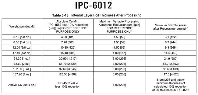
IPC establishes rigorous PCB design standards through documents like IPC-6012, which defines qualification for rigid boards including minimum finished copper. For external layers starting at 1 oz/ft2, it mandates at least 1.0 mil average after processing for general compliance. Internal layers require similar minimums to maintain interlayer reliability. Class 2 boards allow 0.8 mil minimum plating in vias, suiting commercial applications with moderate reliability needs. Class 3 elevates this to 1.0 mil minimum for aerospace or medical uses, ensuring robustness under stress. These specs integrate seamlessly into design workflows, promoting consistent fabrication outcomes.
IPC-2221 complements by providing current capacity charts based on 1.4 mil effective thickness, aiding trace width calculations. Designers reference these for thermal rise predictions under load. Non-compliance risks voiding warranties or field failures. Adhering to IPC ensures interoperability across supply chains.
Comparison with Other PCB Standards
While IPC dominates copper specifications, J-STD-001 addresses assembly processes, requiring compatible plating thicknesses for soldering reliability. It aligns with IPC Class 2/3 minima but emphasizes average barrel wall copper over 75 percent fill in holes. JEDEC standards, often via joint J-STD documents, focus on component-board interactions, specifying test coupons with 2 oz external copper for thermal simulations. IEC guidelines harmonize internationally, referencing equivalent foil weights without deviating from IPC baselines. ASTM contributes material testing methods for foil uniformity, supporting but not overriding thickness minima.
These standards rarely conflict; J-STD supplements IPC for post-fab verification. For instance, JEDEC thermal boards use 2.8 mils finished to mimic power PCBs. Comparing PCB standards reveals IPC as foundational, with others ensuring holistic compliance. Engineers benefit from unified copper weight specifications across documents.
Factors Influencing Copper Thickness Selection
Current requirements dictate thickness; higher amps demand thicker copper to limit voltage drop and heat. Signal speed favors thinner foils for controlled impedance in RF designs. Cost escalates with heavier copper due to extended plating times. Fabrication capabilities limit extremes, like 4 oz/ft2 at 5.5 mils for specialized power boards. Mechanical stability improves with balanced stackups using consistent weights. Simulate thermal profiles early to validate choices.
Layer count affects internals; multilayers often use 0.5 oz internals for density. Vias plating must meet class minima regardless of foil start. Environmental factors like vibration favor Class 3 thicknesses.
Best Practices for PCB Compliance
Specify finished copper in fab drawings, not just starting weight, to align with standards. Use IPC-2221 formulas for trace sizing: width scales inversely with allowable temperature rise. Verify via cross-sections post-plating for plating uniformity. Balance outer and inner weights to prevent warpage during lamination. Prototype high-power designs with 2 oz to confirm current handling.
Document compliance class upfront for quoting accuracy. Collaborate with fabricators on achievable finished mils. Incorporate margin for etching loss in designs.
Practical Insights for Electrical Engineers
In high-frequency applications, 1 oz suffices for impedance control around 50 ohms. Power supplies benefit from 2 oz planes reducing inductance. Troubleshooting thin copper reveals etching overkill; adjust panelization. Hybrid stackups mix weights strategically. Field data shows Class 3 vias lasting 20 percent longer under cycling.
Conclusion
Mastering copper thickness in mils optimizes PCB performance and ensures IPC standards copper thickness adherence. Comparisons highlight IPC's leadership, harmonized by J-STD and JEDEC for full lifecycle compliance. Selecting appropriate weights balances electrical, thermal, and mechanical needs. Engineers achieve reliable designs by prioritizing finished specs and class requirements. This approach upholds PCB design standards, fostering innovation without compromise.
FAQs
Q1: What are the typical IPC standards copper thickness values in mils for standard PCBs?
A1: IPC guidelines specify 1.37 mils nominal for 1 oz/ft2 base foil, with finished external layers around 1.2 mils minimum for Class 2. Internal layers match closely post-lamination. These ensure adequate current capacity per PCB design standards. Always confirm finished values for compliance.
Q2: How do copper weight specifications differ between IPC Class 2 and Class 3?
A2: Class 2 permits 0.8 mil minimum via plating, suiting general electronics, while Class 3 requires 1.0 mil for high-reliability. This impacts PCB compliance in demanding environments. Finished plane thicknesses remain similar but with tighter tolerances in Class 3.
Q3: Why compare PCB standards when IPC dominates copper thickness?
A3: IPC sets core specs, but J-STD-001 verifies assembly plating, enhancing overall reliability. JEDEC aligns for component integration. Comparing PCB standards prevents gaps in copper weight specifications across processes.
Q4: What role does finished copper thickness play in PCB compliance?
A4: Finished thickness post-etching and plating determines real-world performance, per IPC minima. It affects thermal dissipation and via integrity. Specifying it explicitly aids fabricators in meeting standards.
References
IPC-6012E - Qualification and Performance Specification for Rigid Printed Boards. IPC, 2017
IPC-2221B - Generic Standard on Printed Board Design. IPC, 2012
J-STD-001H - Requirements for Soldered Electrical and Electronic Assemblies. IPC/JEDEC, 2018