Introduction
Copper thickness, expressed in mils where one mil equals 0.001 inches, forms the foundation of conductive pathways in printed circuit boards. Engineers must grasp how this parameter interacts with PCB manufacturing tolerances to avoid performance issues in high-reliability applications. Variations during the PCB manufacturing process can alter electrical properties, thermal dissipation, and mechanical integrity. This article delves into copper thickness standards, sources of copper thickness variation, and strategies to navigate PCB fabrication limits. Factory-driven insights reveal how precise control over copper etching and plating steps ensures compliance with industry benchmarks. By understanding these elements, electrical engineers can optimize designs for manufacturability and reliability.
Understanding Copper Thickness in Mils
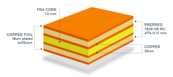
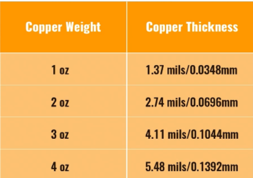
Copper thickness in PCBs originates from the weight of copper foil laminated to the substrate, typically measured in ounces per square foot. A standard 1 oz copper foil corresponds to a nominal thickness of 1.37 mils before processing, while 2 oz doubles that to approximately 2.8 mils. These values represent the starting point in the PCB fabrication process, with final dimensions influenced by subsequent operations. Electrical engineers specify copper weight to balance current-carrying capacity against space constraints, as thicker copper supports higher currents but demands wider traces. Conversion from ounces to mils remains essential for cross-referencing design tools and fabrication drawings.
Factory experience shows that 0.5 oz copper, at about 0.7 mils, suits high-density signal layers, whereas heavier foils like 3 oz find use in power distribution planes. Engineers should note that these are nominal figures, with actual measurements taken via cross-section analysis post-fabrication. Uniformity across the panel affects impedance control and signal integrity in multilayer boards. Selecting the appropriate thickness requires evaluating application demands alongside PCB manufacturing tolerances.
Why Copper Thickness and Tolerances Matter
Precise copper thickness directly impacts trace resistance, where even small deviations amplify heat generation under load. In high-speed designs, copper thickness variation influences characteristic impedance, potentially causing signal reflections if tolerances exceed design margins. PCB manufacturing tolerances ensure that finished boards meet performance specs, preventing field failures in automotive or aerospace systems. Factory processes aim to minimize these variations to uphold reliability across production runs. Engineers who overlook tolerances risk yield losses or requalification costs during prototyping.
Thicker copper enhances mechanical robustness against flexing or vibration, critical for rugged environments. Conversely, thin copper risks fracturing during assembly or operation. Adhering to established PCB fabrication limits maintains consistency between design intent and delivered product. This alignment supports scalable production while mitigating risks from copper etching inconsistencies.
The PCB Manufacturing Process and Sources of Copper Thickness Variation
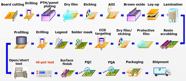
The PCB manufacturing process begins with copper-clad laminates, where foil thickness sets the baseline for conductors. Imaging transfers the pattern, followed by copper etching to remove unwanted material and define traces. Plating then builds up copper in vias and on outer layers, introducing potential non-uniformity. Each step contributes to copper thickness variation, from laminate tolerances to etch depth control. Factories monitor these via statistical process control to stay within PCB manufacturing tolerances.
Laminate suppliers provide copper foils with inherent thickness spreads, often around 10 percent, which propagate through lamination. During etching, the isotropic nature of the process slightly undercuts traces, reducing effective thickness by a few microns. Panel plating versus pattern plating yields different uniformity; panel methods offer better thickness control for outer layers. Environmental factors like etchant temperature and conveyor speed further influence outcomes.
Post-etch cleaning and oxide treatments can erode copper minimally, compounding variations. Multilayer boards face additional challenges during press cycles, where resin flow redistributes pressure on foils. Engineers must account for these in stackup planning to predict final copper profiles accurately.
PCB Fabrication Limits and Copper Etching Considerations
PCB fabrication limits dictate achievable copper thicknesses, typically ranging from 0.5 oz to 6 oz depending on layer count and technology. Thinner foils enable finer features but heighten sensitivity to etching tolerances, while heavy copper demands specialized equipment for uniform removal. Copper etching tolerances control how closely the final trace width matches the artwork, with underetch typically 10 to 20 percent of trace width. These limits stem from chemical kinetics and equipment precision in the PCB manufacturing process.
IPC-6012 outlines qualification requirements for rigid boards, specifying minimum finished copper thicknesses based on starting weight and product class. For instance, outer layer conductors must retain sufficient thickness post-etching to ensure conductivity. Factories calibrate etch lines to balance speed and uniformity, avoiding overetch that thins copper excessively. Plated thicknesses in vias follow similar guidelines, with averages targeted above minimums for margin.
Aspect ratio constraints limit deep plating on heavy copper, capping via depths relative to diameter. Engineers pushing fabrication limits should request capability matrices to align designs. Consistent etchant replenishment minimizes drift over production panels.
Best Practices for Managing Copper Thickness in Design and Production
Specify finished copper thickness explicitly on fabrication drawings to guide process selection. For high-current paths, opt for 2 oz or heavier starting foils, compensating trace widths for etch factor. Pattern plating suits inner layers needing precise buildup, while panel plating excels for outer uniformity. Collaborate with fabricators early to confirm PCB manufacturing tolerances match design needs. Cross-section coupons on panels verify actual thicknesses against specs.
Incorporate IPC-A-600 criteria for acceptance, focusing on conductor thickness measurements at multiple points. Design rules should allocate 20 percent extra width for 1 oz copper etching to absorb variations. Simulate thermal effects using nominal minus minimum thickness for worst-case analysis. Request enhanced controls like tight tolerance plating for critical nets.
Multilayer designs benefit from symmetric stackups to equalize plating stresses. Post-fabrication, automate inspections with X-ray or beta gauges for thickness mapping. These practices reduce copper thickness variation and boost first-pass yields.
Troubleshooting Copper Thickness Variation Issues
Uneven copper thickness often traces to etchant imbalances, manifesting as thicker edges and thinner centers on panels. Cross-check via microsectioning reveals if plating voids contribute. Adjust conveyor speed or chemistry for uniformity in repeat runs. Excessive variation signals foil quality issues; switch suppliers if persistent.
Overetched traces thinning copper below limits fail electrical tests; widen artwork or reduce etch time. Plating inconsistencies in vias stem from poor seed layer coverage; optimize activation steps. Log process parameters to correlate with thickness data for root cause analysis. Factory teams resolve most via SPC charts tracking copper thickness variation.
Conclusion
Mastering copper thickness in mils equips engineers to navigate PCB manufacturing tolerances effectively. From etching to plating, each process step influences final dimensions, underscoring the need for standard-aligned practices. By respecting PCB fabrication limits and specifying thoughtfully, designs achieve reliability without excess cost. Key takeaways include verifying finished thicknesses, compensating for etch effects, and leveraging inspections. Electrical engineers applying these insights ensure robust boards ready for demanding applications.
FAQs
Q1: What are typical PCB manufacturing tolerances for copper thickness?
A1: PCB manufacturing tolerances for copper thickness generally allow 10 to 20 percent variation from nominal, depending on starting weight and class per IPC standards. Factories achieve tighter control through precise etching and plating. Engineers should specify minimum finished thicknesses to account for copper etching losses. This ensures traces meet current ratings reliably.
Q2: How does copper etching affect final thickness in the PCB manufacturing process?
A2: Copper etching removes excess foil isotropically, slightly reducing conductor height while defining widths. Etch factor influences sidewall angles, impacting effective thickness. Factories control this via chemistry and exposure for uniform results. Copper thickness variation here demands design margins for fabrication limits.
Q3: What causes copper thickness variation during PCB fabrication?
A3: Copper thickness variation arises from foil non-uniformity, plating distribution, and process drifts like etchant concentration. Lamination pressures and press cycles add minor contributions in multilayers. Monitoring via coupons mitigates these in production. Adhering to standards minimizes risks.
Q4: How can engineers specify copper thickness to minimize fabrication limits?
A4: Specify starting copper weight and desired finished thickness, noting plating method. Request cross-sections for verification against PCB manufacturing tolerances. Compensate traces for etching tolerances. This factory-driven approach aligns design with process capabilities.
References
IPC-6012E — Qualification and Performance Specification for Rigid Printed Boards. IPC, 2015
IPC-A-600K — Acceptability of Printed Boards. IPC, 2020
J-STD-001H — Requirements for Soldered Electrical and Electronic Assemblies. IPC, 2018