Introduction
Building a weather station as an electronic hobbyist offers a rewarding way to explore environmental monitoring while honing your skills in electronics design. A critical component of this project is creating a custom PCB to integrate sensors, microcontrollers, and power management into a compact, reliable system. This guide walks you through the essentials of designing, laying out, and manufacturing a PCB for your weather station. Whether you are new to PCB design or seeking to refine your skills, this article covers key steps using PCB design software, effective PCB layout techniques, and tips for PCB manufacturing and prototyping. By following industry best practices, you can ensure your weather station operates efficiently and withstands environmental challenges. Let us dive into the process of crafting a tailored PCB solution for your project.
What Is a Custom PCB and Why It Matters for Weather Stations
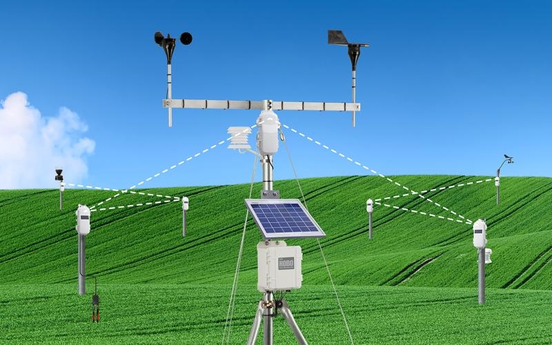
A custom PCB, or printed circuit board, is a tailored electronic platform that connects and supports components like sensors, processors, and power supplies through conductive pathways. Unlike generic breadboards or off-the-shelf modules, a custom PCB allows precise control over component placement, signal integrity, and space efficiency. For a weather station, this means integrating temperature, humidity, pressure, and wind speed sensors into a single, compact unit that can endure outdoor conditions.
The importance of a custom PCB in a weather station lies in its ability to optimize performance and reliability. It reduces wiring clutter, minimizes interference between components, and ensures consistent data collection. Additionally, a well-designed PCB can lower power consumption, which is vital for battery-operated stations in remote locations. For hobbyists, creating a custom PCB also builds valuable skills in electronics design and problem-solving, making it a cornerstone of advanced DIY projects.
Technical Principles of PCB Design for Weather Stations
Designing a PCB for a weather station involves understanding several technical principles to ensure functionality and durability. First, consider the electrical requirements of your components. Weather stations often use low-power sensors and microcontrollers, so the PCB must support appropriate voltage levels and current capacities. Ensure that power traces are wide enough to handle current without excessive heat buildup, following guidelines from industry standards like IPC-2221B for current-carrying capacity.
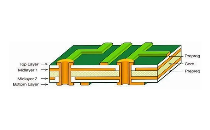
Next, focus on signal integrity. Sensors in weather stations generate analog or digital signals that can be sensitive to noise. Keep signal traces short and away from high-current paths to avoid electromagnetic interference. Ground planes are essential for providing a stable reference and reducing noise, so incorporate them across unused areas of the PCB.
Environmental resilience is another key principle. Weather stations are exposed to moisture, temperature swings, and dust. Select materials and finishes that protect against corrosion, such as conformal coatings, while adhering to standards like IPC-6012E for board performance under stress. Finally, plan for modularity by including connectors for easy sensor replacement or upgrades, ensuring your design remains adaptable for future improvements.
Step-by-Step Guide to Designing a Custom PCB
Choosing the Right PCB Design Software
For hobbyists starting with PCB design, selecting user-friendly software is crucial. Many free or open-source tools offer schematic capture and layout features suitable for beginners. Look for software that supports component libraries, design rule checks, and export options for manufacturing files. Familiarize yourself with basic features like drawing schematics, placing components, and routing traces. Most tools provide tutorials to help you create your first design, ensuring you can draft a weather station PCB with minimal frustration.
Creating the Schematic
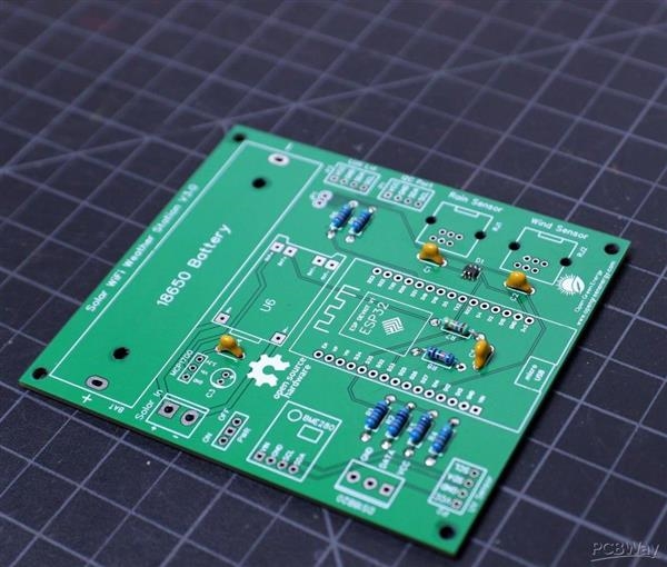
Begin by drafting a schematic, which is a blueprint of your circuit. List all components for your weather station, such as sensors for temperature and humidity, a microcontroller for data processing, and power regulation circuitry. Connect these elements logically, ensuring inputs and outputs match sensor and controller specifications. Include power and ground connections for every component. Double-check your schematic against datasheets to confirm pin assignments and voltage requirements, avoiding errors before moving to the layout phase.
PCB Layout Best Practices
Once the schematic is complete, transition to the PCB layout. Place components strategically, grouping related parts like sensors and their supporting resistors or capacitors together to minimize trace lengths. Position power-hungry components near supply points to reduce voltage drops. Keep sensitive analog traces away from digital signals to prevent interference. Use a ground plane to stabilize signals and reduce noise. Adhere to spacing guidelines from standards like IPC-7351B for component footprints to ensure manufacturability and reliability in your design.
Design Rule Checks and Validation
Before finalizing your layout, run design rule checks to identify errors like overlapping traces or insufficient clearances. These checks ensure your design complies with manufacturing constraints, such as minimum trace widths and spacing. Validate your power distribution network to confirm it meets the needs of all components. If errors arise, revisit your layout or schematic to correct them. This step is critical to avoid costly mistakes during PCB manufacturing and to guarantee a functional prototype.
PCB Manufacturing Basics for Hobbyists
Preparing Files for Manufacturing
After completing your design, export the necessary files for manufacturing, typically in a format like Gerber. These files include layers for copper traces, solder mask, and silkscreen. Include a bill of materials listing all components and a fabrication drawing with board dimensions and special instructions. Verify that your files meet the specifications outlined in standards like IPC-2581 for digital data exchange to ensure compatibility with manufacturing processes.
Understanding PCB Materials and Finishes
For a weather station PCB, material selection impacts durability. Standard FR-4 material suffices for most hobbyist projects due to its balance of cost and performance. However, consider environmental factors like humidity. Opt for a finish that resists corrosion, following guidelines from IPC-4552 for surface finishes. Ensure the chosen materials and finishes align with the expected operating conditions of your weather station to prevent degradation over time.
Ordering Your PCB Prototype
When ready to order a PCB prototype, compile all design files and review them for completeness. Submit your order through a service that offers quick turnaround for small batches, ideal for hobbyists testing designs. Check the proofing options to catch errors before full production. Expect to iterate on your prototype based on testing results, refining the design to address any issues with component fit or electrical performance.
Tips for Building and Testing Your PCB Prototype
Assembly Techniques
Assembling your PCB prototype requires basic soldering skills and tools like a soldering iron and multimeter. Start by placing smaller components like resistors and capacitors before tackling larger ones like connectors. Follow soldering practices from standards like IPC-A-610 for acceptability of electronic assemblies to ensure reliable joints. Work in a clean, static-free environment to avoid damaging sensitive components. Verify each connection visually and with a multimeter to confirm continuity.
Testing and Troubleshooting
Once assembled, power up your weather station PCB and test each sensor output using appropriate software or a serial monitor. Compare readings against expected values to identify discrepancies. If a sensor fails to respond, check solder joints and trace connections for breaks. Use a multimeter to measure voltages at key points, ensuring they match design specifications. Document any issues and revise your design if systemic problems appear, preparing for a second prototype if needed.
Iterating on Your Design
Prototyping often reveals areas for improvement. If testing shows noise in sensor readings, adjust the layout to enhance ground planes or shorten signal paths. If components overheat, reconsider power trace widths or add heat sinks. Each iteration brings your design closer to reliability. Keep detailed notes on changes to track progress and maintain consistency with standards like IPC-6012E for performance specifications during redesigns.
Conclusion
Creating a custom PCB for your weather station as a hobbyist is an achievable and enriching endeavor. By mastering PCB design software, adhering to sound PCB layout practices, and navigating PCB manufacturing and prototyping, you can build a robust platform for environmental monitoring. This guide has outlined the critical steps, from schematic creation to testing, ensuring you have a foundation to develop a reliable system. With attention to technical principles and industry standards, your weather station PCB can deliver accurate data while withstanding challenging conditions. Start small, iterate often, and enjoy the process of bringing your design to life.
FAQs
Q1: How do I choose the best PCB design software for a beginner weather station project?
A1: As a beginner, look for PCB design software with intuitive interfaces and free access to basic features. Ensure it supports schematic capture, layout tools, and design rule checks. Many platforms offer extensive libraries for common components used in weather stations. Tutorials and community support can also ease the learning curve. Take time to explore options that match your skill level and project needs for a smoother design experience. (Alex Chen – PCB Design Expert)
Q2: What are key considerations for PCB layout in a weather station design?
A2: In PCB layout for a weather station, prioritize component grouping to minimize trace lengths and reduce noise. Place sensors away from heat sources and digital signals to maintain accuracy. Use ground planes for stability and follow spacing rules from industry standards. Ensure power traces are adequately sized for current demands. A well-planned layout enhances reliability and data precision in harsh environments. (Alex Chen – PCB Design Expert)
Q3: How can I ensure quality during PCB manufacturing for my prototype?
A3: To ensure quality in PCB manufacturing, verify that your design files are complete and comply with standard formats. Double-check specifications for materials and finishes to suit outdoor conditions. Review manufacturer feedback on your prototype files before production starts. Adhering to guidelines like those for performance specifications helps avoid errors. Clear documentation of your requirements also aids in achieving consistent results. (Sophia Wang – Manufacturing Specialist)
Q4: What challenges might I face when testing a PCB prototype for a weather station?
A4: Testing a PCB prototype for a weather station may reveal issues like sensor inaccuracies due to noise or poor connections. Environmental factors can affect readings if the board lacks proper protection. Power supply inconsistencies might also arise. Use testing tools to measure outputs and inspect solder joints. Systematic troubleshooting and design iteration will help resolve these challenges effectively. (Grace Li – Assembly Engineer)
References
IPC-2221B — Generic Standard on Printed Board Design. IPC, 2012.
IPC-7351B — Generic Requirements for Surface Mount Design and Land Pattern Standard. IPC, 2010.
IPC-6012E — Qualification and Performance Specification for Rigid Printed Boards. IPC, 2020.
IPC-A-610H — Acceptability of Electronic Assemblies. IPC, 2020.
IPC-4552A — Specification for Electroless Nickel/Immersion Gold (ENIG) Plating for Printed Boards. IPC, 2017.
IPC-2581C — Generic Requirements for Printed Board Assembly Products Manufacturing Description Data and Transfer Methodology. IPC, 2021.


