Introduction
For electronic hobbyists venturing into advanced circuit board projects, mastering via-in-pad PCB design opens up new possibilities for compact and efficient layouts. This technique, often used in high-density designs, allows vias to be placed directly within component pads, saving valuable board space and enhancing signal integrity. Whether you are working on a DIY project or prototyping a complex device, learning to design a via-in-pad PCB can elevate your skills. In this guide, we will walk through the essentials of via-in-pad technology, its benefits, and a detailed step-by-step process to make your first via-in-pad PCB. Tailored for hobbyists, this article focuses on easy PCB design methods to help you achieve professional results with limited resources. Let us dive into the world of hobbyist PCB design and explore this innovative approach.
What Is Via-in-Pad PCB Design and Why It Matters
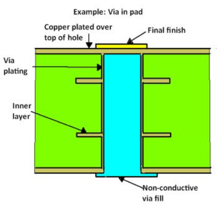
Via-in-pad refers to a PCB design technique where a via, a small hole that connects different layers of a circuit board, is placed directly inside a component's pad. Unlike traditional vias positioned outside pads, this method integrates the via into the pad itself, often filled or capped for a seamless connection. This approach is particularly valuable in high-density interconnect designs where space is limited, such as in modern smartphones or compact IoT devices.
The significance of via-in-pad PCB design lies in its ability to reduce board size and improve electrical performance. By eliminating the need for additional routing space, hobbyists can create smaller, more efficient layouts. Additionally, it minimizes signal path lengths, which enhances signal integrity, a critical factor in high-speed circuits. For DIY via-in-pad PCB projects, this technique also simplifies assembly for fine-pitch components like ball grid arrays. Understanding and applying this method can set your hobbyist PCB design apart, making it a skill worth mastering.
Technical Principles Behind Via-in-Pad Design
To grasp via-in-pad PCB design, it is essential to understand its core principles. A via is typically a plated through-hole that electrically connects different layers of a PCB. In a via-in-pad setup, this hole is drilled directly into the pad where a component lead or ball will be soldered. To prevent solder wicking into the via during assembly, these vias are often filled with conductive or non-conductive material and capped with a thin layer of metal, as per industry practices outlined in standards like IPC-4761.
The primary advantage is space optimization. Traditional vias require a separate annular ring and clearance area, consuming additional board space. Via-in-pad eliminates this need, allowing tighter component placement. Electrically, it reduces parasitic inductance due to shorter connection paths, which is vital for high-frequency signals. However, challenges include potential manufacturing defects if not designed correctly, such as voids in via filling or misalignment, which can affect reliability. Adhering to guidelines from standards like IPC-6012E ensures that your design meets quality expectations for hobbyist PCB design projects.
Related Reading: Enhancing PCB Reliability with Via in Pad Technology
Step-by-Step Guide to Design Via-in-Pad PCB
Creating your first via-in-pad PCB as a hobbyist requires careful planning and attention to detail. Below is a structured process to help you design and make a via-in-pad PCB, tailored for easy PCB design with DIY tools and resources.
Step 1: Understand Your Project Requirements
Begin by assessing your project needs. Identify components that benefit from via-in-pad, such as fine-pitch integrated circuits or ball grid arrays. Determine the layer count of your PCB, as via-in-pad is often used in multilayer boards. Ensure your design goals align with space constraints and performance needs, which are common in hobbyist PCB design.
Step 2: Select Appropriate Design Software
Choose a PCB design tool suitable for hobbyists that supports via-in-pad configurations. Many free or low-cost options allow manual via placement within pads. Familiarize yourself with the software's via settings to define parameters like drill size and pad dimensions, following guidelines from standards like IPC-7351B for land pattern design.
Step 3: Define Via and Pad Specifications
Set the via size based on your board's layer thickness and manufacturing capabilities. Typically, microvias or small-diameter vias are used in via-in-pad designs to fit within pads. Ensure the pad is large enough to accommodate the via without compromising solderability. Refer to IPC-6012E for performance specifications to avoid issues like insufficient annular ring or via breakout.
Step 4: Place Vias Within Pads
In your design software, place the via directly inside the component pad. Ensure alignment with the component footprint to prevent connection issues. If your software supports it, enable via filling or capping options to indicate this requirement for manufacturing. Proper placement is critical to avoid signal interference or assembly defects in your DIY via-in-pad PCB.
Step 5: Route Traces and Verify Connections
Route traces to connect the via-in-pad to other layers or components as needed. Keep trace lengths short to maintain signal integrity, especially for high-speed signals. Use design rule checks to verify that vias do not violate spacing or clearance rules, adhering to best practices for easy PCB design.
Step 6: Add Design Notes for Manufacturing
Include clear documentation in your design files to inform the fabrication house of via-in-pad requirements. Specify whether vias should be filled with conductive or non-conductive material and capped, as per IPC-4761 guidelines. Clear instructions reduce the risk of errors during production of your hobbyist PCB design.
Step 7: Review and Finalize Design
Before sending your design for fabrication, perform a thorough review. Check for via-to-pad alignment, ensure no overlapping errors, and confirm compliance with manufacturing tolerances. Use simulation tools if available to predict signal performance. A meticulous review ensures a successful outcome when you make a via-in-pad PCB.
Step 8: Choose a Fabrication Service
Select a PCB fabrication service that supports via-in-pad technology. Many services catering to hobbyists offer advanced features like via filling for multilayer boards. Provide detailed notes and confirm their capabilities to handle your DIY via-in-pad PCB requirements without compromising quality.
Best Practices for Hobbyist Via-in-Pad PCB Design
To achieve reliable results in your via-in-pad PCB projects, follow these best practices tailored for hobbyists working on easy PCB design.
- Start with simple designs. Focus on small projects with fewer components to practice via-in-pad placement before tackling complex layouts.
- Use standard via sizes. Stick to common drill diameters that most fabrication services can handle to avoid production delays or extra costs.
- Prioritize signal integrity. Place vias in pads strategically to minimize interference, especially for sensitive analog or high-speed digital signals.
- Communicate with fabricators. Clearly state via-in-pad needs in your design files to ensure they understand filling and capping requirements as per IPC-4761.
- Test prototypes thoroughly. After receiving your boards, inspect vias and solder joints for defects to learn from any issues in your DIY via-in-pad PCB.
Common Challenges and Troubleshooting Tips
Even with careful planning, hobbyists may encounter issues when designing a via-in-pad PCB. One frequent problem is solder wicking, where solder flows into an unfilled via, causing poor connections. To prevent this, ensure vias are specified for filling and capping during fabrication. Another issue is misalignment between vias and pads, which can lead to assembly failures. Double-check your design files using design rule checks to catch such errors early.
If you notice poor signal performance in your prototype, verify that trace routing around via-in-pad areas avoids sharp bends or unnecessary length. For manufacturing defects like incomplete via filling, consult your fabricator to confirm their process aligns with standards like IPC-6012E. Keeping a log of issues and solutions will refine your skills in hobbyist PCB design over time.
Related Reading: Troubleshooting Common Via-in-Pad Issues in PCB Design
Conclusion
Designing your first via-in-pad PCB as an electronic hobbyist is a rewarding step toward creating compact and high-performing circuit boards. By understanding the principles behind this technique, following a structured design process, and adhering to industry standards, you can achieve professional-quality results in your DIY via-in-pad PCB projects. This guide has provided actionable steps and best practices to simplify via-in-pad PCB design, ensuring that even beginners can tackle this advanced method. With practice and attention to detail, you will master easy PCB design and unlock new potential in your electronic creations.
FAQs
Q1: What are the benefits of via-in-pad PCB design for hobbyists?
A1: Via-in-pad PCB design offers space savings and improved signal integrity, making it ideal for hobbyists working on compact projects. It allows tighter component placement, reducing board size, which is perfect for DIY via-in-pad PCB builds. Additionally, shorter signal paths minimize interference in high-speed circuits. With proper planning, hobbyists can leverage this technique to create efficient, professional-grade designs.
Q2: How can I ensure my DIY via-in-pad PCB is manufactured correctly?
A2: To ensure your DIY via-in-pad PCB is made correctly, provide detailed design notes specifying via filling and capping needs. Reference standards like IPC-4761 for via protection methods. Communicate with your fabricator to confirm they support this technology. Review their capabilities and request a prototype to check for issues before full production.
Q3: What tools are best for hobbyist PCB design with via-in-pad features?
A3: For hobbyist PCB design, choose user-friendly software that supports via-in-pad placement and offers design rule checks. Many free or affordable tools provide features to define via sizes and pad dimensions as per IPC-7351B. Focus on platforms with community support for tutorials and troubleshooting to make via-in-pad PCB design easier.
Q4: Are there risks in using via-in-pad for easy PCB design projects?
A4: Yes, risks in via-in-pad for easy PCB design include solder wicking if vias are not filled, or misalignment causing connection issues. These can be mitigated by adhering to standards like IPC-6012E and verifying designs before fabrication. Hobbyists should start with simple layouts to minimize errors while learning this advanced technique.
References
IPC-6012E — Qualification and Performance Specification for Rigid Printed Boards. IPC, 2020.
IPC-4761 — Design Guide for Protection of Printed Board Via Structures. IPC, 2006.
IPC-7351B — Generic Requirements for Surface Mount Design and Land Pattern Standard. IPC, 2010.


