Introduction
Printed Circuit Boards (PCBs) form the backbone of modern electronics, and their design directly impacts the functionality, durability, and affordability of electronic devices. Among the many design parameters, PCB thickness stands out as a critical factor influencing performance, cost, and reliability. Engineers and designers often face the challenge of balancing these aspects to meet application-specific needs. Whether it is ensuring signal integrity in high-speed circuits or maintaining structural integrity in rugged environments, PCB thickness optimization plays a pivotal role. This article explores the technical principles behind PCB thickness, its impact on design outcomes, and practical strategies for achieving the best results. Aimed at electrical engineers, this guide provides structured insights to inform design decisions for various applications.
What Is PCB Thickness and Why It Matters
PCB thickness refers to the total height of the board, typically measured in millimeters or inches, encompassing the substrate, copper layers, and any additional coatings or finishes. Standard thicknesses often range between 0.4 mm and 3.2 mm, depending on the application and manufacturing constraints. The choice of thickness affects multiple aspects of a PCB, including mechanical strength, thermal management, and electrical performance.
For electrical engineers, understanding the implications of PCB thickness is essential. A thinner board may reduce material costs and fit compact designs, but it could compromise durability. Conversely, a thicker board might enhance reliability in harsh conditions but increase production expenses. Optimizing PCB thickness is about finding the right balance for specific project requirements, ensuring the board performs well without unnecessary costs or risks.
Technical Principles Behind PCB Thickness
Impact on Electrical Performance
PCB thickness influences electrical characteristics such as impedance control and signal integrity, especially in high-frequency applications. The dielectric layer's thickness between copper traces affects the capacitance and, consequently, the signal propagation speed. In multilayer boards, consistent thickness ensures uniform impedance across layers, which is critical for maintaining signal quality. Standards like IPC-2221B, which provides guidelines for PCB design, emphasize the importance of controlled dielectric spacing for electrical performance.
Additionally, thickness impacts current-carrying capacity. Thicker boards can accommodate wider traces or heavier copper weights, supporting higher currents without excessive heat buildup. This is particularly relevant for power electronics where thermal dissipation is a concern. Engineers must consider these factors during PCB thickness design to avoid signal loss or overheating issues.
Mechanical Strength and Durability
From a mechanical perspective, PCB thickness directly correlates with the board's ability to withstand physical stress. Thinner boards are more prone to warping or cracking under mechanical loads or during assembly processes like soldering. Standards such as IPC-6012E outline performance specifications for rigid PCBs, including requirements for structural integrity based on thickness and material properties.
In applications like automotive or aerospace, where vibration and shock are common, a thicker PCB often provides better reliability. However, excessive thickness can lead to challenges in fitting the board into tight enclosures or increase weight, which is undesirable in portable devices. Balancing mechanical needs with design constraints is a key aspect of PCB thickness optimization.
Thermal Management Considerations
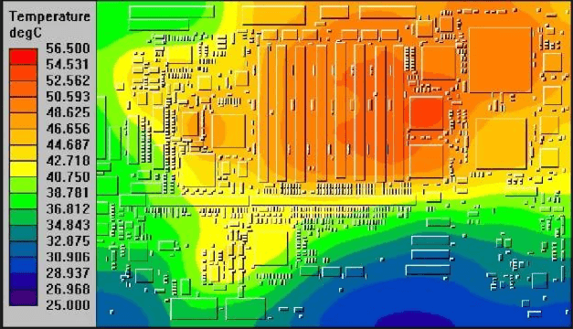
Thermal performance is another critical area influenced by PCB thickness. Thicker boards generally have better heat dissipation capabilities due to a larger mass to absorb and distribute thermal energy. This is vital in high-power applications where components generate significant heat. However, thicker boards may also retain heat longer, potentially affecting component longevity if not managed properly.
Conversely, thinner boards may struggle with heat dissipation, leading to localized hot spots. Engineers often rely on thermal vias or heat sinks to mitigate these issues, but the board's thickness remains a foundational factor. Guidelines from IPC-2222A for sectional design standards help in determining appropriate thickness for thermal perfor mance in specific use cases.
Suggested Reading: The Impact of MCPCB Thickness on Thermal Performance and Mechanical Stability
Practical Strategies for PCB Thickness Optimization
Assessing Application Requirements
The first step in optimizing PCB thickness is to evaluate the specific needs of the application. For consumer electronics, where space and cost are primary concerns, thinner boards around 0.8 mm to 1.2 mm are often sufficient. In contrast, industrial or military applications may require thicker boards, such as 2.0 mm or more, to ensure reliability under harsh conditions. Understanding the operating environment, including temperature ranges and mechanical stress, guides the selection process.
Engineers should also consider the component density and type. High-density designs with fine-pitch components may benefit from thinner boards to reduce parasitic effects, while power-intensive designs might need thicker substrates for better current handling. Aligning thickness with application demands ensures a balanced approach to PCB thickness performance.
Balancing Cost and Material Selection
Cost is a significant factor in PCB thickness design. Thicker boards require more raw material, increasing production expenses. Additionally, manufacturing processes for thicker boards can be more complex, especially in multilayer configurations, leading to higher labor and equipment costs. Standards like IPC-A-600K provide acceptability criteria for printed boards, helping engineers specify thickness without over-engineering, thus controlling expenses.
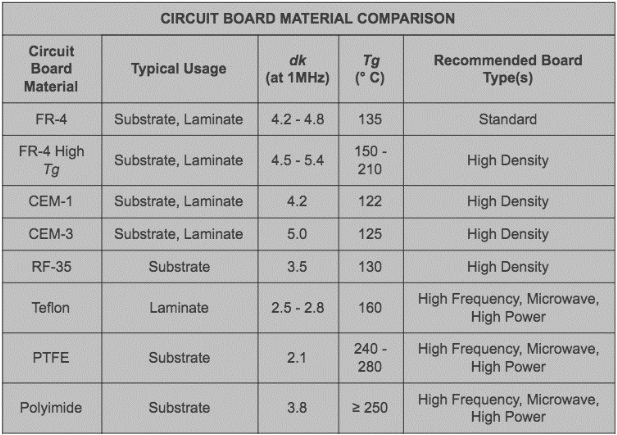
Material choice also plays a role in cost optimization. Common substrates like FR-4 vary in price based on their thickness and grade. Selecting a material that meets performance needs without exceeding budget limits is crucial. Engineers can use design guidelines from IPC-4101D, which covers laminate specifications, to choose cost-effective options while maintaining reliability.
Design for Manufacturability
Optimizing PCB thickness for manufacturability reduces production errors and ensures consistent quality. Thinner boards, while cost-effective, can be challenging to handle during fabrication and assembly due to their flexibility. Conversely, very thick boards may require specialized equipment for drilling or lamination, increasing lead times. Adhering to manufacturing tolerances outlined in IPC-6012E helps in selecting a thickness that aligns with standard processes.
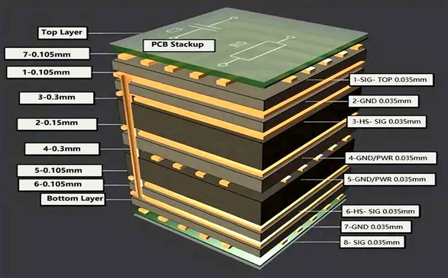
Engineers should also account for stackup design in multilayer PCBs. Uniform layer distribution and appropriate dielectric thickness prevent issues like warpage or delamination. Tools and guidelines from IPC-2221B assist in creating manufacturable designs that balance PCB thickness cost and reliability.
Testing and Validation
Validation through testing is essential to confirm that the chosen PCB thickness meets performance and reliability goals. Mechanical tests, such as bend and flex assessments, evaluate the board's durability under stress. Thermal cycling tests, guided by standards like JEDEC J-STD-020E, assess how thickness impacts heat resistance and component solder joint integrity.
Electrical testing, including impedance measurements, ensures that the thickness supports signal integrity requirements. Incorporating these tests into the design phase helps identify potential issues early, allowing for adjustments before full-scale production. This proactive approach enhances PCB thickness reliability for long-term use.
Insight: Common Challenges in PCB Thickness Selection
One frequent challenge in PCB thickness optimization is misalignment between design intent and manufacturing capabilities. Engineers might specify a non-standard thickness to achieve specific performance goals, only to find that it complicates fabrication or increases costs. Consulting standards like IPC-2222A during the design phase can prevent such discrepancies by aligning specifications with common practices.
Another issue is underestimating environmental impacts. A board designed with minimal thickness for cost savings might fail prematurely in high-vibration settings. Conducting thorough environmental simulations and referencing guidelines from IPC-6012E ensures that the chosen thickness withstands real-world conditions without compromising PCB thickness performance.
Conclusion
Optimizing PCB thickness is a multifaceted process that requires careful consideration of performance, cost, and reliability. By understanding the technical principles behind thickness, such as its effects on electrical, mechanical, and thermal properties, engineers can make informed decisions tailored to specific applications. Practical strategies, including application assessment, cost balancing, manufacturability design, and thorough testing, provide a roadmap for achieving optimal results. Adhering to established industry standards ensures that designs meet quality and consistency benchmarks. Ultimately, PCB thickness design is about striking a balance that supports functionality while minimizing expenses and risks, ensuring robust and efficient electronic systems.
FAQs
Q1: How does PCB thickness affect performance in high-speed designs?
A1: PCB thickness impacts signal integrity in high-speed designs by influencing impedance and capacitance. Thicker dielectric layers can alter signal propagation, potentially causing delays or losses. Following design standards like IPC-2221B helps maintain consistent impedance. Engineers must select an appropriate thickness to minimize parasitic effects and ensure reliable data transmission.
Q2: What factors influence PCB thickness cost during production?
A2: PCB thickness cost is driven by material usage, manufacturing complexity, and layer count. Thicker boards require more substrate material and may need specialized processes, increasing expenses. Standards like IPC-A-600K guide engineers in specifying thickness that balances cost with quality, avoiding over-specification while meeting application needs.
Q3: How can PCB thickness reliability be ensured for harsh environments?
A3: PCB thickness reliability in harsh environments depends on mechanical strength and thermal resilience. Thicker boards often withstand vibration and shock better, as outlined in IPC-6012E. Environmental testing, including thermal cycling per JEDEC J-STD-020E, validates durability. Matching thickness to operating conditions is critical for long-term performance.
Q4: What role does PCB thickness optimization play in thermal management?
A4: PCB thickness optimization is vital for thermal management as it affects heat dissipation. Thicker boards can absorb and distribute heat more effectively, preventing hot spots in high-power applications. Referencing IPC-2222A for sectional design helps select a thickness that supports thermal needs without compromising other design goals.
References
IPC-2221B - Generic Standard on Printed Board Design. IPC, 2012.
IPC-2222A - Sectional Design Standard for Rigid Organic Printed Boards. IPC, 2010.
IPC-6012E - Qualification and Performance Specification for Rigid Printed Boards. IPC, 2020.
IPC-A-600K - Acceptability of Printed Boards. IPC, 2020.
IPC-4101D - Specification for Base Materials for Rigid and Multilayer Printed Boards. IPC, 2014.
JEDEC J-STD-020E - Moisture/Reflow Sensitivity Classification for Nonhermetic Surface Mount Devices. JEDEC, 2014.


