Introduction
FR-4 serves as the foundational material in most rigid printed circuit boards, enabling reliable performance across electronics applications. Electric engineers often encounter FR-4 in designs requiring balanced mechanical strength, electrical insulation, and cost-effectiveness. Understanding the FR-4 PCB fabrication process demystifies how design files transform into functional boards through precise, sequential operations. This guide outlines the core steps, from lamination to silkscreen, highlighting engineering considerations at each stage. Factory-driven insights reveal how these processes ensure compliance with quality benchmarks, minimizing defects like delamination or plating voids. By grasping these mechanisms, engineers can optimize designs for manufacturability and reliability.
What Is FR-4 and Why It Matters
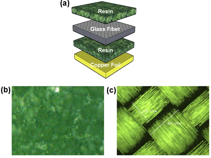
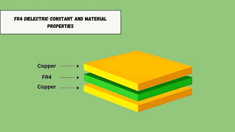
FR-4 refers to a grade of flame-retardant fiberglass epoxy laminate, composed of woven E-glass fabric impregnated with brominated epoxy resin. This composite provides high mechanical stability, with a glass transition temperature typically suited for standard soldering processes. Its dielectric properties support signal integrity in multilayer boards, making it ideal for consumer electronics, automotive controls, and industrial systems. In the PCB manufacturing process, FR-4 acts as both core and prepreg, bonding copper layers while insulating circuits. Engineers value FR-4 for its process compatibility, allowing high-volume production without exotic handling. Deviations in material quality directly impact bow and twist, underscoring the need for consistent sourcing aligned with base material specifications.
The ubiquity of FR-4 stems from its balance of performance and economy, dominating over 90 percent of rigid PCB production. It withstands thermal cycling during assembly, yet requires careful process control to avoid issues like cafing or z-axis expansion. For electric engineers, specifying FR-4 influences stackup planning, impedance control, and thermal management from the outset.
The FR-4 PCB Fabrication Process: Step-by-Step
Inner Layer Preparation and Etching
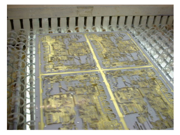
Multilayer FR-4 PCB fabrication begins with inner layer cores, where copper-clad FR-4 panels undergo surface preparation for imaging. Dry film photoresist laminates onto cleaned copper foils, followed by precise alignment of phototools under UV exposure. The exposed resist hardens, while developer removes unexposed areas, revealing unwanted copper for etching. Chemical etchants, such as ferric chloride or cupric solutions, dissolve exposed copper, defining trace patterns down to fine geometries. Post-etch inspection verifies line width and spacing, with resist stripping via alkaline solutions completing the cycle. This step demands tight registration to prevent misalignment during subsequent lamination.
Factory processes often include oxide treatment, like black oxide or reduction, to enhance prepreg adhesion and prevent inner layer exposure.
Lamination
Lamination bonds processed inner layers with B-stage prepreg sheets and outer copper foils into a unified stackup. Optical punching or pin registration ensures layer-to-layer alignment within microns. The assembly enters a vacuum-assisted press, where controlled heat, typically 170 to 190 degrees Celsius, and pressure, around 300 to 500 psi, cure the epoxy resin. Flow control in prepreg fills vias and bonds interfaces, forming a rigid FR-4 structure with specified thickness tolerance. Post-lamination, x-ray verification confirms registration accuracy before proceeding. Dimensional stability here prevents warpage, critical for high-density interconnects.
This process adheres to qualification specs for rigid boards, ensuring interlayer bonds withstand mechanical stress.
Drilling
Drilled holes create vias and component through-holes, starting with CNC-controlled mechanical drills for standard aspect ratios up to 10:1. Entry and backup materials protect the FR-4 stack from burrs and delamination at drill entry and exit. Laser drilling supplements for microvias in advanced FR-4 boards, ablating precise barrels without mechanical force. Post-drill deburring employs chemical or plasma methods to smooth edges. Aspect ratio limits dictate stackup feasibility, with deeper holes risking incomplete plating later. Engineers must account for drill wander in design, specifying clearances accordingly.
Plating
Desmear processing follows drilling, using permanganate solutions to etch resin smear from hole walls, ensuring uniform plating adhesion. Electroless copper deposits a catalytic seed layer, typically 0.5 to 1 micron thick, rendering barrels conductive. Panel electroplating then builds copper thickness, often 20 to 30 microns, via electrolytic baths with anode current control. A tin or tin-lead flash overplates traces, acting as etch resist for outer layers. Plating uniformity prevents dog-boning or overplating, verified by cross-section analysis. This sequence interconnects layers electrically, foundational to FR-4 functionality.
Outer Layer Etching
Outer layers mirror inner processing post-plating, with photoresist imaging defining final circuitry. Etching removes excess copper, protected by tin, using similar chemistries as inner layers. Tin stripping via peroxide or nitric solutions exposes pure copper traces. Precise conveyor speed and spray patterns control undercut, maintaining critical dimensions. Electrical test post-etch detects opens or shorts early. Alignment with plated vias ensures signal integrity continuity.
Solder Mask Application
Liquid photoimageable solder mask (LPSM) coats the etched board, providing insulation and solder dam control. Screen printing or curtain coating applies uniform thickness, followed by UV exposure through photomask. Development clears openings at pads and vias, with thermal cure hardening the mask. This layer prevents bridging during assembly and protects traces from oxidation. Mask adhesion testing confirms durability under thermal shock. Colorants, often green, aid visual inspection without affecting properties.
Silkscreen Printing
Silkscreen adds legend markings using epoxy-based inks pushed through emulsion-coated stencils. Alignment fixtures ensure polarity symbols, references, and fab notes register accurately. UV or thermal curing solidifies ink, resistant to solvents and soldering. White ink contrasts against solder mask for readability. This non-functional layer supports assembly and rework, with opacity preventing bleed-under. Final visual checks precede surface finish.
Best Practices for FR-4 PCB Fabrication
Engineers should design within process capabilities, specifying drill sizes per IPC class and avoiding blind vias unless justified. Stackup symmetry minimizes warpage, with balanced copper distribution aiding flatness. Process controls like automated optical inspection after etching catch defects early. For plating, maintain bath chemistry to avoid skips, cross-sectioning samples routinely. Solder mask tenting over vias enhances reliability, while silkscreen font heights ensure legibility post-reflow. Adhering to acceptability criteria optimizes yield and field performance.
Acceptability standards guide visual and dimensional checks throughout.
Conclusion
The FR-4 PCB fabrication process integrates etching, plating, drilling, lamination, solder mask, and silkscreen into a cohesive workflow, transforming epoxy-glass sheets into robust interconnects. Each step builds on the prior, demanding precision to achieve electrical and mechanical integrity. Electric engineers benefit from this knowledge, refining designs to leverage FR-4 strengths while mitigating limitations. Factory insights emphasize process sequencing and controls for consistent outcomes. Ultimately, mastering these steps elevates PCB reliability in demanding applications.
FAQs
Q1: What role does etching play in the FR-4 PCB fabrication process?
A1: Etching selectively removes unwanted copper after photoresist patterning, defining traces and pads on inner and outer layers. It uses controlled chemical solutions to undercut minimally, preserving line widths. Post-etch stripping and inspection ensure cleanliness. This step is pivotal for multilayer alignment and fine-pitch features. Proper conveyor etching prevents over-etch, aligning with quality specs.
Q2: How does lamination contribute to FR-4 multilayer boards?
A2: Lamination fuses inner cores, prepreg, and foils under heat and pressure, curing resin for interlayer bonds. Vacuum assists in void-free stacking, critical for via reliability. Registration tools maintain alignment tolerances. Post-lamination thickness control supports impedance planning. It sets the foundation for subsequent drilling and plating.
Q3: Why is plating essential after drilling in PCB manufacturing process?
A3: Plating metallizes hole walls, creating vertical interconnects between FR-4 layers. Electroless seeding enables electrolytic buildup for conductivity. Uniform thickness avoids high-resistance paths. Desmear precedes to ensure adhesion. This interconnects circuits reliably across the stackup.
Q4: What are key considerations for solder mask and silkscreen in FR-4 fabrication?
A4: Solder mask insulates traces, defining solderable areas via photoimaging. It cures to withstand reflow temperatures. Silkscreen follows, adding durable markings for assembly. Both enhance protection and usability without electrical impact. Alignment and thickness uniformity prevent defects.
References
IPC-6012E — Qualification and Performance Specification for Rigid Printed Boards. IPC, 2017
IPC-A-600K — Acceptability of Printed Boards. IPC, 2020
IPC-4101 — Specification for Base Materials for Rigid and Multilayer Printed Boards. IPC, 2017