Introduction
Aluminum printed circuit boards represent a critical advancement in thermal management for power electronics applications. These boards feature a metal core that efficiently dissipates heat from high-power components such as power transistors, diodes, and capacitors. In power supplies, inverters, and motor drives, where heat generation is substantial, aluminum PCBs prevent thermal runaway and extend component life. Designers must address unique challenges like electrical isolation, current handling, and high-voltage spacing to ensure reliability. This article explores aluminum PCB design rules, focusing on high voltage aluminum PCB requirements, current capacity in aluminum PCBs, creepage and clearance aluminum PCB considerations, and isolation requirements power electronics. By adhering to established engineering principles, engineers can optimize performance in demanding environments.
Why Aluminum PCBs Matter in Power Electronics
Power electronics operate under high currents and voltages, generating significant joule heating and switching losses. Traditional FR-4 boards struggle with thermal conductivity around 0.3 W/mK, leading to hotspots and derating of components. Aluminum PCBs, with base thermal conductivity exceeding 200 W/mK, spread heat uniformly to integrated heatsinks or chassis. This capability supports higher power densities in applications like DC-DC converters and electric vehicle inverters. Moreover, the mechanical rigidity of the aluminum core reduces warpage during thermal cycling, enhancing long-term reliability. Selecting aluminum substrates aligns with the need for compact, efficient designs in modern power systems.
Fundamental Structure and Material Properties
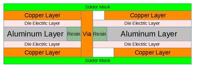
Aluminum PCBs consist of three primary layers: a copper circuit layer, a thermally conductive dielectric, and an aluminum base plate. The copper layer, typically 1 to 3 oz/ft2 thick, carries signals and power traces. The dielectric layer, often 75 to 150 μm thick, provides electrical isolation while maintaining high thermal transfer, usually above 1 W/mK. The aluminum base, 1 to 3 mm thick, acts as a heat spreader and mounting platform. Material selection influences voltage withstand, with dielectrics rated for breakdown strengths over 10 kV/mm. Engineers must balance thickness for isolation against thermal resistance to avoid hotspots under load.
Thermal Management Principles
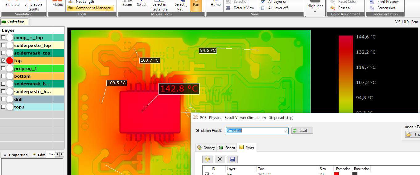
Effective thermal design begins with understanding heat flow paths in aluminum PCBs. Heat from components conducts through the copper, dielectric, and into the aluminum base before dissipating via convection or conduction to external sinks. Finite element analysis helps predict junction temperatures, ensuring they stay below component limits. Via stitching under high-power devices enhances lateral heat spreading within the copper layer. The aluminum core's high diffusivity minimizes temperature gradients across the board. Adhering to IPC-2221B guidelines for thermal vias and pad sizing supports robust heat dissipation strategies.
Current Capacity in Aluminum PCBs
Current capacity in aluminum PCBs depends on trace width, copper thickness, and ambient temperature rise. Thicker copper foils enable higher amperage without excessive heating, as the aluminum base aids cooling. IPC-2152B provides methodologies for calculating trace widths based on cross-sectional area and allowable temperature rise. For power electronics, traces carrying tens of amperes require widths exceeding 5 mm for 2 oz copper at 20°C rise. Plating and surface finishes affect skin effect at high frequencies, influencing AC current limits. Designers simulate combined copper and base conduction for accurate ratings, preventing electromigration in prolonged operation.
In practice, wide traces or solid copper pours maximize current handling while minimizing voltage drops. The aluminum substrate reduces overall trace temperatures compared to standard boards, allowing 20-50% higher capacities under forced airflow. Edge effects and board curvature must be factored in for non-planar designs. Integrating current sensors verifies performance during prototyping. These considerations ensure aluminum PCBs meet demands in high-current paths of inverters and rectifiers.
High Voltage Aluminum PCB Design Challenges
High voltage aluminum PCBs demand meticulous attention to electric field distribution and partial discharge risks. Voltages exceeding 500 V accentuate the need for robust dielectric integrity between traces and the grounded base. Surface contamination on the aluminum can initiate tracking, so clean manufacturing processes are essential. Voltage standoff capability hinges on dielectric thickness and material comparative tracking index per IEC 60664-1. Engineers specify coatings or potting for added protection in humid environments. Finite element modeling of fields around sharp corners prevents corona inception.
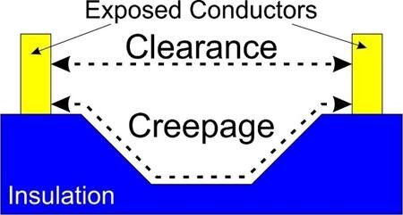
Creepage and Clearance in Aluminum PCBs
Creepage and clearance distances prevent arcing and surface tracking in high voltage aluminum PCBs. Creepage measures the shortest path along the insulation surface between conductors, while clearance is the straight-line air path. IEC 60664-1 defines minimum values based on working voltage, pollution degree, and material group. For 1000 V systems at pollution degree 2, creepage might require 8 mm on standard surfaces. Grooves, barriers, or conformal coatings extend effective creepage paths on aluminum substrates. Trace routing avoids right angles near high-voltage nodes to reduce field crowding.
In power electronics, primary-to-secondary isolation in switchers exemplifies these rules. Clearance ensures flashover resistance, scaled by altitude and overvoltage categories. Aluminum's conductivity necessitates slotted bases to interrupt creepage paths to chassis grounds. Verification via hi-pot testing confirms compliance post-assembly. These aluminum PCB design rules safeguard against failures in variable environments.
Isolation Requirements in Power Electronics
Isolation requirements power electronics prioritize galvanic separation between input, output, and control circuits. The dielectric layer in aluminum PCBs provides primary isolation to the heatsink, typically rated for 2-5 kV AC. Multi-layer configurations or embedded capacitors enhance functional isolation. Optocouplers and transformers demand surrounding clearance per safety standards. Partial discharge inception voltage guides dielectric selection for long-term reliability. Ground plane partitioning minimizes common-mode noise coupling.
Secondary isolation via slots in the aluminum base prevents unintended current paths. Voltage rating must exceed peak transients from switching. Thermal expansion mismatch between layers requires flexible dielectrics to avoid cracks. Testing per IPC-6012 standards validates isolation under humidity and temperature swings. These practices ensure safe, reliable operation in isolated power topologies.
Practical Aluminum PCB Design Rules and Best Practices
Aluminum PCB design rules start with stackup definition, specifying layer thicknesses and copper weights early. Minimum trace-to-trace spacing follows IPC-2221B for voltage and current density. Annular rings around vias prevent cracking during thermal stress. Component placement prioritizes heat sources near board edges for optimal sinking. Solder mask over bare aluminum edges protects against corrosion. Fabrication tolerances for base milling accommodate heatsink mating.
For assembly, thermal pads or paste fill gaps between components and base. Multiple mounting holes distribute mechanical stress evenly. Design for testability includes isolated test points for hi-pot. Iterative simulation refines layouts before prototyping. Documentation of design rules streamlines revisions.
In high-power inverters, symmetric routing balances currents and reduces EMI. Current capacity calculations incorporate derating for elevation. Creepage enhancers like molded barriers suit compact designs. Post-design reviews against standards catch oversights.
Applications and Troubleshooting Insights
In switch-mode power supplies, aluminum PCBs handle resonant converters efficiently. Inverters benefit from direct chassis integration, eliminating separate heatsinks. Troubleshooting hotspots involves infrared thermography to identify dielectric voids. Warpage from asymmetric heating requires balanced copper distribution. High-voltage breakdowns trace to contamination, resolved by plasma cleaning.
Conclusion
Designing aluminum PCBs for power electronics integrates thermal, electrical, and mechanical considerations for peak performance. Key aluminum PCB design rules encompass current capacity optimization, creepage and clearance aluminum PCB spacing, and robust isolation requirements power electronics. High voltage aluminum PCB challenges yield to standards-guided practices. Engineers achieve reliable, high-density boards by prioritizing simulation, material selection, and verification. These strategies enable advancements in efficient power conversion systems.
FAQs
Q1: What are the primary aluminum PCB design rules for current capacity in aluminum PCBs?
A1: Aluminum PCB design rules for current capacity emphasize thick copper foils and wide traces per IPC-2152B methodologies. The aluminum base enhances cooling, supporting higher densities than FR-4. Calculate widths for specified temperature rises, incorporating airflow. Verify with thermal modeling to prevent hotspots in power paths.
Q2: How do creepage and clearance aluminum PCB requirements differ in high voltage applications?
A2: Creepage and clearance aluminum PCB distances follow IEC 60664-1, scaled by voltage and pollution degree. Creepage accounts for surface paths, often extended via slots on the metal base. Clearance prevents air breakdown. Coatings increase effective distances in humid conditions. High voltage aluminum PCB designs prioritize these for safety isolation.
Q3: What isolation requirements power electronics impose on aluminum PCBs?
A3: Isolation requirements power electronics demand dielectrics with high breakdown strength between circuits and the aluminum base. Ratings exceed working voltages by safety margins. Slots and barriers provide secondary isolation. Testing ensures endurance under transients. This setup supports galvanic separation in converters and inverters.
Q4: Why is thermal management critical in high voltage aluminum PCB design?
A4: Thermal management prevents dielectric degradation in high voltage aluminum PCB designs. Heat reduces isolation strength, risking partial discharge. Aluminum cores spread heat effectively, maintaining uniform temperatures. Integrate vias and sinks per design rules. Monitoring sustains reliability in power electronics.
References
IPC-2221B — Generic Standard on Printed Board Design. IPC, 2003
IPC-2152B — Standard for Determining Current Carrying Capacity in Printed Board Design. IPC, 2009
IEC 60664-1 — Insulation coordination for equipment within low-voltage systems — Part 1: Principles, requirements and tests. IEC, 2007
IPC-6012DS — Qualification and Performance Specification for Rigid Printed Boards with Double-Sided or Multilayer Copper Metallization. IPC, 2015


