Why is Harmonizing PCB Size and Enclosure Design So Important?
The symbiotic relationship between the dimensions of a Printed Circuit Board (PCB) and its protective enclosure is a fundamental aspect of successful electronic product development. A poorly conceived enclosure can lead to a cascade of problems, including an ill-fitting board, thermal management issues, or undue mechanical stress on components. Conversely, a meticulously planned design guarantees robust protection from environmental elements, simplifies the assembly process, and significantly enhances the end-user experience.
Fundamental Design Considerations
Key elements to address early in the design cycle include precisely matching the PCB's dimensions to the enclosure, meticulously planning mounting points, and accounting for all components that project from the board, such as various connectors or heat sinks. By tackling these considerations upfront, designers can circumvent costly redesigns, avoid production delays, and ensure a streamlined manufacturing process.
What Are the Key Factors in PCB and Enclosure Design Integration?
Achieving an ideal fit between your quick turn PCB and its housing demands close attention to several critical factors. Let’s systematically explore these elements.
1. Determining Accurate PCB Dimensions
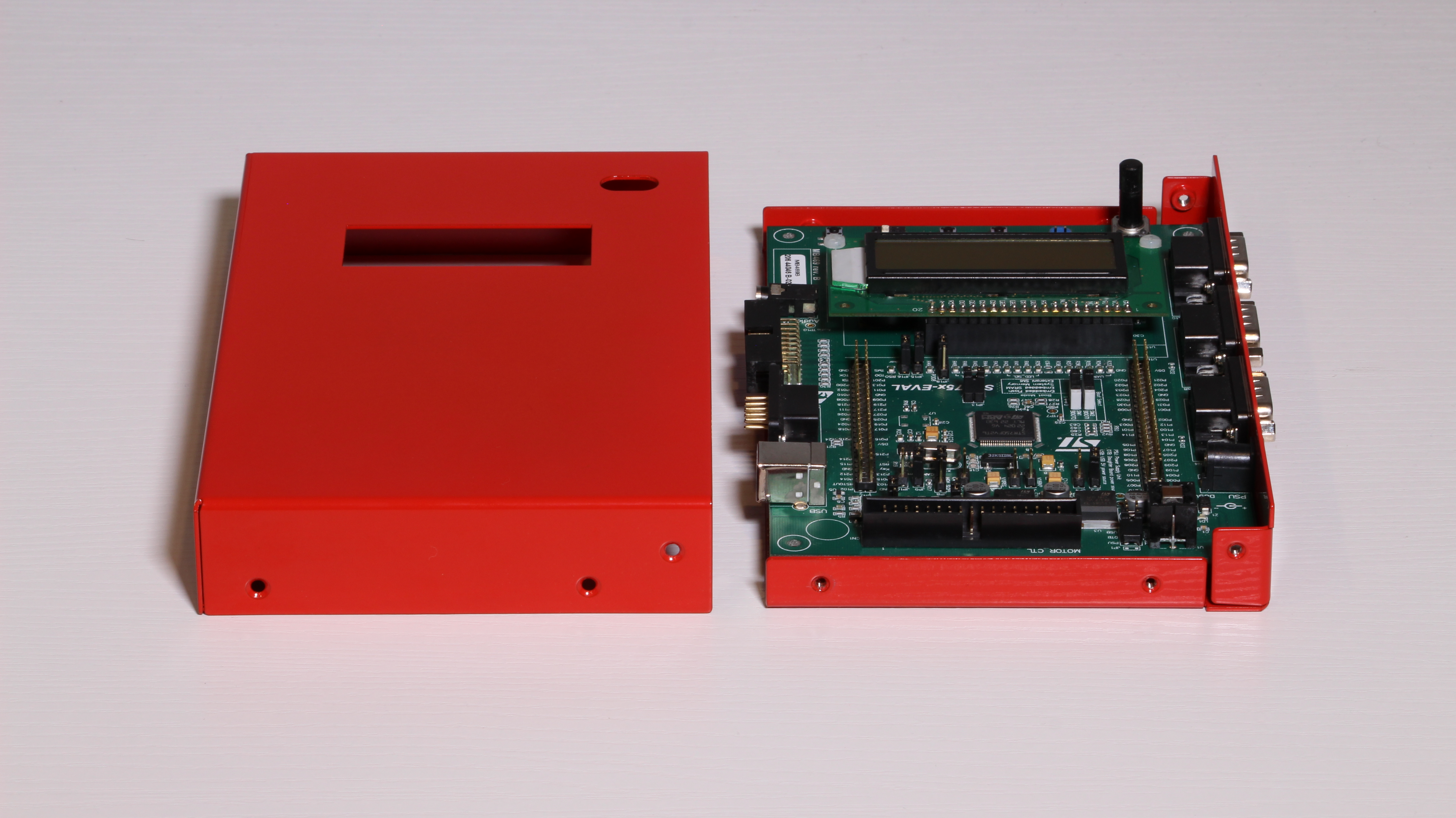
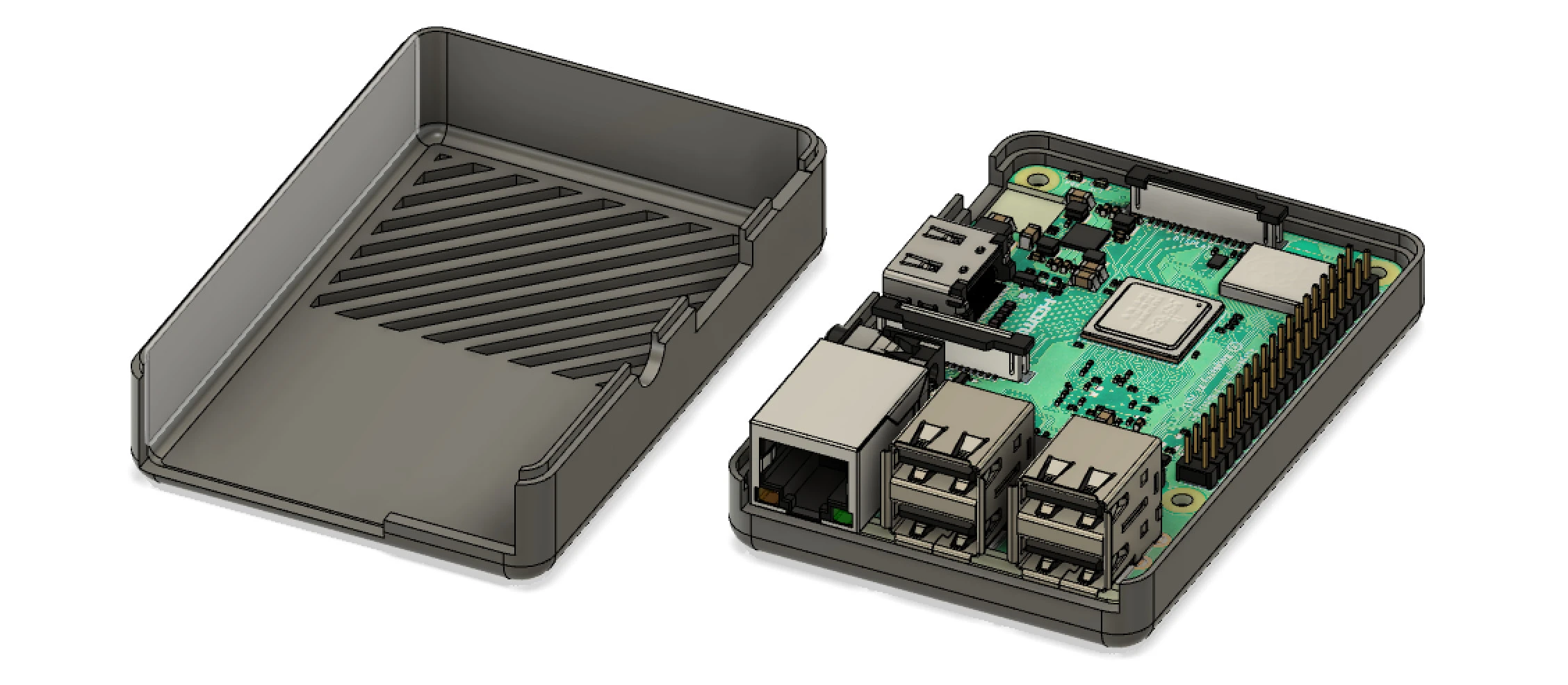
The initial step in integrating PCB size with enclosure design involves accurately defining the board's dimensions. This extends beyond simple length and width; it necessitates considering the vertical clearance required for components and any irregular shapes or cutouts on the board. For instance, if your PCB incorporates tall capacitors or heat sinks, the enclosure must provide adequate overhead clearance—typically 2-3 mm above the tallest component—to prevent contact or undesirable mechanical stress during assembly.
Start by creating a precise layout of your PCB, meticulously noting the position of every component. Leveraging design software to generate a 3D model, if possible, greatly aids in visualizing the spatial requirements. Standard PCB thicknesses range from 0.8 mm to 1.6 mm, though custom boards may vary. Ensure the enclosure design accounts for this specific thickness when planning mounting features or slots.
2. Aligning Enclosure Dimensions with PCB Size
Once your PCB dimensions are finalized, the next crucial step is selecting or designing an enclosure with corresponding internal dimensions. A common pitfall is choosing an enclosure that is too restrictive, leaving insufficient space for cabling, connectors, or essential ventilation. A practical guideline is to incorporate at least 5-10 mm of additional clearance around the PCB's perimeter to comfortably accommodate wiring and manufacturing tolerances during assembly.
For example, if a PCB measures 100 mm by 80 mm, an enclosure with internal dimensions of at least 110 mm by 90 mm would be appropriate. Furthermore, factor in the thickness of the enclosure walls—typically 1-3 mm for plastic enclosures and 2-5 mm for metal ones—when calculating the final external dimensions.
3. Strategizing for Secure PCB Mounting
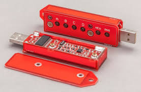
Effective PCB mounting is a pivotal aspect of enclosure design, guaranteeing that the board remains firmly secured throughout its operational life. Common mounting techniques include using screws with standoffs, snap-in clips, or integrated rail systems. The optimal method depends heavily on the specific application and its environmental demands.
● Screws and Standoffs: This is the most prevalent and secure mounting approach. Employ standoffs with a height of 3-6 mm to elevate the PCB from the enclosure's base, thereby preventing potential short circuits. Ensure that the mounting holes on the PCB (typically 3.2 mm in diameter for M3 screws) perfectly align with the corresponding mounting points within the enclosure.
● Snap-in Clips: Ideal for rapid assembly, these clips are frequently employed in plastic enclosures. However, they may not be suitable for applications involving high vibration.
● Rail Systems: Often found in industrial settings, systems like DIN rails facilitate quick and easy installation and removal of PCBs.
When designing for mounting, it's prudent to avoid positioning components too close to the mounting holes, as this can induce undesirable mechanical stress. Maintaining a minimum clearance of 5 mm around each mounting hole is considered a good design practice.
4. Addressing PCB Design Specific Constraints
Every project is shaped by a unique set of PCB design constraints that influence both the board and enclosure design. These constraints can encompass diverse factors such as electrical performance requirements, thermal management needs, and environmental operational conditions.
● Electrical Constraints: High-speed circuitry may necessitate specific trace widths and spacing to preserve signal integrity. For instance, a 50-ohm impedance trace for RF applications might require a width of 0.5 mm on a standard 1.6 mm thick FR4 PCB board. Ensure the enclosure design does not introduce interference with these sensitive traces by avoiding conductive materials in close proximity to critical areas.
● Thermal Management: Efficient heat dissipation is critical for high-power components. If your PCB includes a power regulator dissipating, for example, 5W of heat, the enclosure should incorporate vents or be fabricated from a thermally conductive material such as aluminum. Allow at least 10 mm of clear space around major heat-generating components to facilitate adequate airflow.
● Environmental Factors: For devices intended for outdoor use, the enclosure must provide robust protection against ingress of dust and water. Select enclosures rated IP65 or higher for such demanding applications, and ensure the PCB layout avoids exposed traces that could be susceptible to corrosion.
What Mechanical Design Factors Ensure a Perfect PCB-Enclosure Fit?
Beyond electrical and dimensional considerations, the mechanical design plays a crucial role in achieving a flawless fit. This involves strategic planning for physical stresses, ease of assembly, and the user's interaction with the final product.
1. Enclosure Material Selection
The choice of material for the enclosure directly impacts both the product's functionality and its manufacturing cost. Common materials include:
● Plastics: Lightweight and cost-effective, plastic enclosures are frequently used in consumer electronics. Materials like ABS plastic offer good impact resistance and are easily molded into custom shapes. However, they may not be suitable for high-temperature environments (above 80°C).
● Metals: Aluminum or steel enclosures provide exceptional durability and effective EMI (Electromagnetic Interference) shielding, making them ideal for industrial applications. While heavier and more expensive, they can withstand temperatures up to 150°C or higher.
Select the enclosure material based on the specific mechanical and environmental stresses your project will encounter. For example, a handheld device would prioritize a lightweight plastic enclosure, whereas a factory control unit would require a robust metal one.
2. Designing for Streamlined Assembly and Maintenance
A thoughtfully designed enclosure not only perfectly houses the PCB but also facilitates straightforward assembly and maintenance procedures. Consider the following elements:
● Accessible Points: Ensure the enclosure provides unhindered access to all connectors, buttons, or displays located on the PCB. Cutouts must align with precision to the PCB components—tolerances of ±0.2 mm are often necessary for a professional and functional finish.
● Secure Fastening Mechanisms: Utilize screws, clips, or hinges that allow the enclosure to be opened and closed without risking damage to the PCB. Avoid designs that necessitate excessive force during assembly, as this can impart undue stress on the board.
● Organized Cable Management: Allocate adequate internal space for neat cable routing. A chaotic internal wiring setup can lead to signal interference or mechanical damage over time.
3. Mitigating Mechanical Stress
Mechanical stress, whether from vibration, impact, or improper mounting, can severely damage a PCB. To mitigate these risks, consider reinforcing the enclosure with internal ribs or thicker walls in areas prone to high stress. Furthermore, incorporating shock-absorbing materials like rubber gaskets between the PCB and its mounting points can effectively dampen vibrations, particularly in demanding automotive or industrial applications where vibration frequencies can range from 10 Hz to 200 Hz.
What Are the Best Practices for Seamless PCB and Enclosure Integration?
To conclude, here are some essential best practices that will guide you in harmonizing PCB size and enclosure design for a perfect, functional fit.
● Leverage 3D Modeling Tools: Software with integrated electrical and mechanical design capabilities can simulate the PCB's fit within the enclosure, allowing you to identify and rectify potential issues virtually before committing to physical manufacturing.
● Prototype and Thoroughly Test: Always create a physical prototype to meticulously test the fit and functionality. Even minor misalignments, such as a 0.5 mm offset in mounting holes, can lead to significant problems during the final assembly stage.
● Account for Manufacturing Tolerances: Be aware that manufacturing tolerances for both PCBs and enclosures can vary (typically ±0.1 to ±0.3 mm). Design with these variations in mind to prevent overly tight fits that complicate assembly.
● Prioritize Effective Ventilation: If your PCB generates considerable heat, ensure the enclosure incorporates strategically positioned vents or slots to maximize airflow without compromising the structural integrity of the housing.
● Maintain Comprehensive Documentation: Keep meticulous records of all dimensions, material selections, and key design decisions. This detailed documentation will prove invaluable for any future revisions, troubleshooting, or product iterations.
Conclusion
Designing a PCB and its enclosure to fit together flawlessly demands meticulous planning, precise measurements, and a deep understanding of both electrical and mechanical engineering principles. By keenly focusing on PCB size and enclosure design, optimizing enclosure dimensions, ensuring secure PCB mounting, addressing all pertinent PCB design constraints, and incorporating robust mechanical design principles, you can create an electronic product that is not only functional and durable but also possesses a professional finish.
Begin with accurate dimensional data, make informed material selections, and rigorously test your design. By adhering to these steps, you will successfully navigate common design pitfalls and ensure that your PCB and its enclosure operate in perfect harmony, delivering a reliable and high-quality solution for your project’s specific requirements.


