Introduction
Single-sided printed circuit boards remain a cornerstone in cost-sensitive electronics applications due to their simplicity and reliability. Designing these boards with manufacturability in mind ensures smoother production transitions, higher yields, and reduced costs. Electric engineers often overlook subtle design choices that impact fabrication until prototypes reveal issues. By adhering to established single-sided PCB design rules, teams can avoid common pitfalls like routing conflicts or assembly complications. This article explores structured approaches to optimize single-sided PCB layouts for production. It provides logical guidance drawn from industry standards to support efficient workflows.
What Is a Single-Sided PCB and Why Design for Manufacturability Matters
A single-sided PCB features conductive traces and pads on only one side of the insulating substrate, typically with components mounted on the same copper-clad surface. This configuration limits routing to a single plane, eliminating vias and multilayer complexities. Such boards excel in low-density circuits like consumer gadgets, LED displays, and basic control systems where space and budget constraints dominate. Design for manufacturability (DFM) integrates fabrication and assembly considerations early, preventing defects that arise from incompatible layouts. Without DFM focus, engineers risk extended lead times, scrap rates, and redesign cycles. Prioritizing DFM aligns design intent with production capabilities, enhancing overall project success.
In high-volume scenarios, single-sided PCBs benefit from streamlined etching and drilling processes, but poor design amplifies issues like trace shorts or solder bridging. Standards like IPC-2221 outline baseline requirements for conductor sizing and spacing to maintain integrity across classes. Electric engineers targeting manufacturability evaluate trade-offs between functionality and producibility from schematic capture onward. This proactive stance minimizes iterations and supports scalable output.
Key Technical Principles in Single-Sided PCB Design
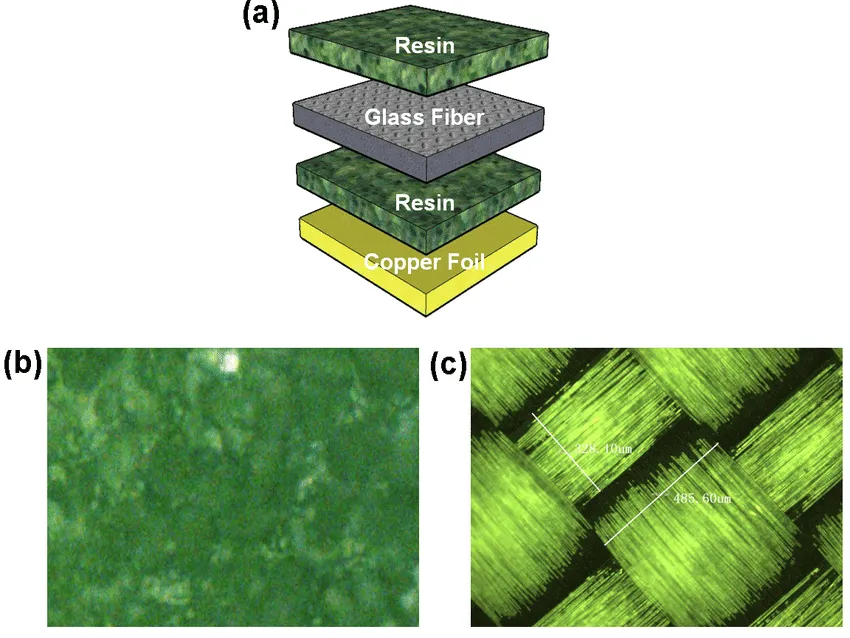
The core principle of single-sided PCB design revolves around planar routing, where all interconnections occur on one copper layer without vertical transitions. Substrate materials like FR-4 provide mechanical stability, but thermal expansion coefficients demand careful pad and trace dimensioning to prevent delamination. Conductor paths must accommodate current densities without excessive heating, following guidelines for width versus amperage. Clearance between traces prevents arcing or etching undercuts during fabrication. Component footprints require sufficient land areas for reliable soldering, balancing density with accessibility.
Routing topology influences signal integrity and manufacturability; serpentine or meandering paths increase resistance and potential for defects. Jumpers, if unavoidable, should bridge non-critical sections to avoid high-current crossings. Panelization principles apply even to single-sided boards, ensuring fiducials and breakaway tabs facilitate batch processing. Adherence to IPC-6011 performance specs verifies qualification across environmental stresses. These mechanisms underpin robust designs that transition seamlessly to production.
Essential Single-Sided PCB Design Rules
Single-sided PCB design rules emphasize minimum feature sizes tailored to fabrication tolerances. Conductor widths scale with current load to mitigate voltage drops and hotspots, while spacings safeguard against bridging during solder application. Annular rings around pads ensure robust plating adhesion if through-hole components appear, though non-plated holes suffice for most surface-mount needs. Hole diameters align with lead sizes, incorporating drill-to-copper margins for repeatability. Edge-to-copper distances prevent board warping or exposure during routing.
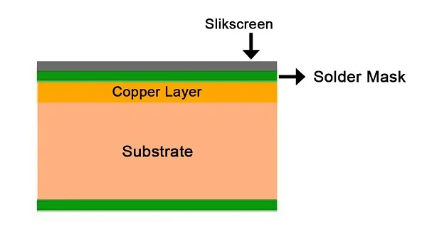
Silkscreen and solder mask layers demand clear definitions to avoid overlaps that complicate inspection. Mask openings match pad geometries precisely, preventing solder wicking onto traces. Polarity markings and reference designators enhance assembly accuracy without cluttering the layout. These rules, rooted in IPC-2221, form the foundation for reliable boards across product classes. Deviations require engineering justification and process validation.
Practical Best Practices for Single-Sided PCB Layout
Start with schematic review to cluster components by function, minimizing trace lengths and jumper dependencies. Place high-power elements near edges for heat dissipation, ensuring airflow paths remain unobstructed. Route traces orthogonally, favoring 45-degree angles over 90-degree bends to reduce etch variability. Group signals to isolate analog from digital sections, preserving noise margins on the shared plane. Incorporate test points at key nodes for in-circuit verification without compromising density.
Solder mask expansion rules prevent exposure of fine-pitch traces during reflow. Silkscreen legends should use fonts with adequate stroke widths for legibility post-fabrication. For prototypes, include coupon areas for material testing, though production panels optimize space. These practices streamline transitions from design to fab, aligning with factory capabilities.
Single-Sided PCB Design Software Free Options and Tutorials
Electric engineers can leverage free single-sided PCB design software to prototype layouts adhering to core rules. These tools support schematic entry, auto-routing constrained to one layer, and Gerber exports for fab houses. Follow a single-sided PCB design tutorial to set layer stackups, define design rules, and generate drill files. Tutorials emphasize DRC checks for spacing violations and panelization previews. Open-source platforms enable iterative refinement without licensing costs, ideal for validation.
Practice importing netlists and adjusting footprints for single-layer constraints. Export ODB++ or standard formats ensure compatibility. Such workflows build proficiency in DFM-integrated design.
Single-Sided PCB Design Review Checklist
A comprehensive single-sided PCB design review checklist verifies manufacturability before submission. Confirm all nets connect without jumps exceeding board thirds. Verify trace widths meet current requirements per class. Check pad-to-pad clearances exceed minimums, with no acute angles under 45 degrees. Inspect solder mask and paste layers for overlaps or undersizing.
Evaluate silkscreen for readability and non-overlap with masks. Ensure fiducials position correctly for automated handling. Review panelization for v-scoring or tab breaks. Flag mirrored layers or incorrect copper side designations. IPC-A-600 criteria guide visual acceptability post-fab. Finalize with BOM cross-check for lead form factors.
Checklist Item: Trace Width & Spacing — Pass Criteria: Per IPC-2221 class — Notes: Measure all conductors
Checklist Item: Pad Annular Ring — Pass Criteria: Adequate for drill — Notes: No less than spec
Checklist Item: Solder Mask Clearance — Pass Criteria: 0.1mm expansion typical — Notes: No trace exposure
Checklist Item: Silkscreen Legibility — Pass Criteria: Bold fonts, no overlap — Notes: Post-mask view
Checklist Item: Jumper Usage — Pass Criteria: Minimal, non-critical — Notes: Alternative routing?
Checklist Item: Panel Features — Pass Criteria: Fiducials, breaks — Notes: Batch compatible
Troubleshooting Common Issues in Single-Sided Designs
Engineers encounter routing deadlocks when nets cross unavoidably, resolved by logical grouping or wire bridges. Warpage from asymmetric copper distribution warps boards; balance pour areas judiciously. Solder bridging plagues dense pads, mitigated by mask dams and stencil apertures. Etch factor variations widen inner traces; compensate with rule adjustments. Post-assembly shorts trace to mask misalignment; validate layer alignments early.
These insights stem from production feedback loops, refining future iterations.
Conclusion
Mastering single-sided PCB design rules elevates prototypes to production-ready boards. Logical adherence to principles like planar routing and DFM checklists curtails defects and accelerates timelines. Free tools and tutorials democratize access for electric engineers honing skills. Standards ensure consistency across classes, from consumer to industrial. Implement these best practices to optimize yield and cost. Future designs benefit from iterative reviews, fostering manufacturable excellence.
FAQs
Q1: What are the core single-sided PCB design rules for beginners?
A1: Single-sided PCB design rules prioritize minimum trace widths, spacings, and pad sizes per IPC-2221 guidelines for the product class. Route all paths on one layer, avoiding unnecessary jumps. Ensure solder mask clearances prevent bridging. Balance copper to minimize warpage. These rules support reliable fabrication and assembly.
Q2: How can I find single-sided PCB design software free for tutorials?
A2: Free single-sided PCB design software abounds online, supporting basic rule checks and Gerber output. A single-sided PCB design tutorial guides layer setup and routing constraints. Practice DRC runs to validate layouts. Export files match fab requirements seamlessly. Start with simple schematics to build confidence.
Q3: What does a single-sided PCB design review checklist include?
A3: A single-sided PCB design review checklist covers trace integrity, mask alignments, silkscreen clarity, and panel features. Verify net connectivity and jumper minimization. Check annular rings and edge clearances. Confirm IPC compliance visually. Address issues pre-submission to boost yield.
Q4: Why focus on DFM in single-sided PCB design?
A4: DFM in single-sided PCB design reduces fabrication rejects from etch errors or assembly shorts. It optimizes routing for one-layer limits, cutting costs. Standards like IPC-A-600 ensure acceptability. Early checks prevent costly respins. This approach scales prototypes effectively.
References
IPC-2221B — Generic Standard on Printed Board Design. IPC, 2003
IPC-A-600H — Acceptability of Printed Boards. IPC, 2010
IPC-6011D — Generic Performance Specification for Printed Boards. IPC, 2015