Why is 50 ohm impedance a crucial factor in modern PCB design?
In the realm of high-frequency and radio frequency (RF) applications, maintaining a precise impedance, typically 50 ohms, is paramount for optimal signal transmission. This 50-ohm standard is widely adopted across RF systems because it strikes an excellent balance between managing power and minimizing signal loss, making it ideal for devices such as antennas, amplifiers, and various communication modules. Neglecting proper impedance control can lead to detrimental signal reflections, substantial power loss, and a significant degradation in circuit performance.
Designing a PCB stackup to achieve 50 ohm impedance necessitates a meticulous approach, involving careful selection of materials, precise calculation of trace dimensions, and a thoughtful arrangement of layers. These elements must work in concert to deliver the desired impedance characteristics. We will delve into the critical aspects of this process, providing insights to help you create reliable and efficient designs.
What are the fundamental principles of 50 ohm impedance in PCBs?
Impedance within a PCB refers to the opposition encountered by the flow of alternating current (AC) signals as they travel along a conductive trace. For high-frequency RF signals, a consistent 50-ohm impedance ensures smooth signal propagation from the source to the load, largely free from reflections. When impedance mismatches occur, standing waves can form, leading to energy dissipation and suboptimal system performance.
Two primary transmission line structures are commonly employed in PCBs to achieve a controlled 50 ohm impedance: microstrip and stripline. Microstrip traces are situated on the outer layers of the PCB, with a dedicated ground plane directly beneath them. In contrast, stripline traces are embedded within internal layers, sandwiched between two ground planes. Each configuration possesses distinct characteristics and demands specific design considerations, which we will explore in detail.
What key factors influence 50 ohm impedance in PCB stackup design?
Achieving 50 ohm impedance in a PCB stackup demands careful consideration of several interconnected factors, including the arrangement of layers, the geometry of signal traces, and the inherent properties of the materials used. Here, we break down the critical elements that must be addressed during the design phase.
Strategic Layer Stackup Configuration
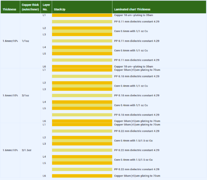
The layer stackup defines the total number of layers in your PCB and their precise arrangement. For effective 50 ohm impedance control, a multi-layer PCB, typically comprising four or more layers, is commonly utilized. This allows for the integration of dedicated ground planes and precise placement of signal traces. A typical four-layer stackup might include:
● Top Layer: Reserved for critical signals (often microstrip traces).
● Layer 2: A dedicated Ground Plane, serving as a reference.
● Layer 3: A Power Plane, for stable power distribution.
● Bottom Layer: May contain additional signals or another Ground Plane.
The ground plane's proximity to a microstrip trace or its enveloping of a stripline trace is vital for establishing impedance. Maintaining a consistent dielectric thickness between the signal layer and its reference ground plane is paramount for uniform impedance across the entire board.
Dielectric Constant (Dk) and Material Selection
The dielectric material situated between the PCB layers significantly impacts signal propagation speed and, consequently, impedance. The dielectric constant (Dk) of this material dictates how much the signal's velocity is reduced as it traverses the PCB. For designs requiring 50 ohm impedance, materials with a stable Dk value, typically ranging between 3.5 and 4.5, are preferred. Common material choices include standard FR-4 for more economical designs and specialized high-frequency laminates such as Rogers or Isola for superior performance in demanding RF applications.
When selecting a PCB material for 50 ohm impedance, consider:
● Low Loss Tangent: Materials exhibiting a low loss tangent minimize signal attenuation, especially at higher frequencies.
● Thermal Stability: The material must maintain its electrical properties consistently across a range of operating temperatures.
● Cost vs. Performance Trade-off: Balance the need for high-performance, often more expensive, materials against project budget constraints.
Trace Width, Spacing, and Copper Thickness
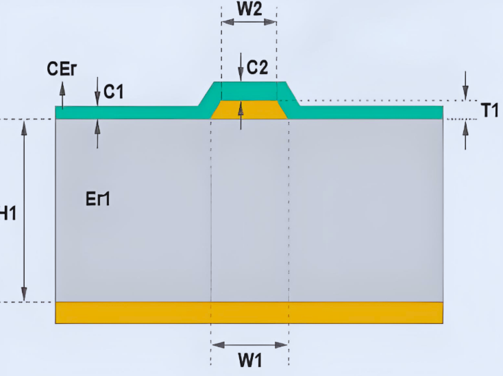
The dimensions of the signal trace—specifically its width (W), thickness (T), and its distance from the ground plane(s) (H or B)—directly determine the characteristic impedance. For a microstrip line, a wider trace generally results in lower impedance, while a narrower trace leads to higher impedance. Similarly, the dielectric thickness separating the trace from its reference ground plane is a critical variable. In stripline designs, where the trace is encased between two ground planes, the precise spacing between these planes (B) must be rigorously controlled.
As a general guideline, for a common 4-layer PCB utilizing FR-4 material (with a Dk of approximately 4.2), a microstrip trace width of about 6-8 mils and a dielectric thickness of 5-6 mils can help achieve 50 ohm impedance. However, these values are highly dependent on specific material properties and the overall stackup configuration, necessitating accurate calculations or simulation.
How are microstrip and stripline impedances calculated for 50 ohm designs?
Accurately calculating the impedance of transmission lines is a fundamental step in achieving precise 50 ohm control. These calculations depend on the physical dimensions of the trace and the electrical properties of the PCB materials.
Microstrip Impedance Calculation
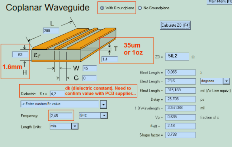
For a microstrip trace, which resides on an outer layer with a single ground plane beneath it, the impedance (Z₀) is determined by the trace width (W), the dielectric thickness (H) between the trace and ground, the trace thickness (T), and the dielectric constant (Dk) of the substrate. While complex formulas exist, here's a commonly used simplified approximation:
Z₀ ≈ (87 / √(Dk + 1.41)) * ln(5.98 * H / (0.8 * W + T))
For example, on a PCB with a 6-mil dielectric thickness, a 1.4-mil trace thickness, and a Dk of 4.2, adjusting the trace width to approximately 7 mils might yield 50 ohm impedance. However, relying solely on manual calculations can be prone to inaccuracies. Utilizing specialized simulation tools or online calculators is highly recommended for greater precision and to accommodate the nuances of your specific stackup.
Stripline Impedance Design
Stripline configurations are often chosen for their superior shielding capabilities and reduced crosstalk, as the trace is fully embedded between two ground planes. Here, the impedance (Z₀) depends on the trace width (W), the overall distance between the ground planes (B), the trace thickness (T), and the dielectric constant (Dk). A simplified formula for stripline impedance is:
Z₀ ≈ (60 / √Dk) * ln(4 * B / (0.67 * π * (0.8 * W + T)))
Consider a multilayer PCB with a Dk of 4.2 and a 10-mil spacing between ground planes. To achieve 50 ohm impedance, the trace width might be around 4-5 mils. Stripline designs are generally more challenging to fabricate due to their internal placement but offer enhanced signal integrity crucial for demanding high-frequency applications.
What are the best practices for designing an impedance-controlled layer stack?
Designing an impedance-controlled layer stack requires a meticulous, systematic approach to ensure consistent performance and manufacturability. Adhering to these best practices will help optimize your 50 ohm impedance PCB stackup.
Strategic Layer Arrangement and Symmetry
● Maintain Symmetry: Aim for a symmetrical stackup whenever possible. This minimizes the risk of board warpage during manufacturing and ensures uniform thermal expansion, which is beneficial for long-term reliability.
● Dedicated Ground Planes: Always place ground planes directly adjacent to signal layers that require impedance control. These planes provide a stable and consistent return path for signals, which is fundamental for maintaining uniform impedance.
Minimizing Discontinuities and Validating Design
● Minimize Via Transitions: Vias, which connect traces between layers, can act as impedance discontinuities, particularly at high frequencies. Employ techniques like back-drilling or using blind/buried vias for high-speed signals to reduce the length of unused via stubs, thereby mitigating reflections.
● Simulate and Test: Always use electromagnetic field simulation software to model your proposed stackup and verify impedance values before sending the design for fabrication. Post-fabrication, perform Time Domain Reflectometer (TDR) testing on actual boards to confirm that the achieved impedance closely matches your design targets.
Collaborating for Material Selection
● Work with Manufacturers: Engage with your online PCB manufacturer early in the design process. They can offer invaluable insights into material availability, suggest optimal stackup configurations for manufacturability, and provide data sheets for specific dielectric materials. This collaboration ensures your material choices and stackup design are both feasible and cost-effective.
What common challenges arise in 50 ohm impedance design and how can they be addressed?
Designing for precise 50 ohm impedance often presents several hurdles. Understanding these common issues and their respective solutions is key to successful high-frequency PCB development.
Addressing Material Variations
● Challenge: Dielectric constants (Dk) can exhibit slight variations between different batches of PCB laminates, leading to unintended impedance shifts.
● Solution: Specify tight tolerances for dielectric thickness and Dk values with your PCB manufacturer. Requesting material certifications can also help ensure consistency.
Managing Trace Etching Accuracy
● Challenge: Inaccuracies during the PCB manufacturing process, such as over-etching or under-etching of copper traces, can alter the intended trace widths and, consequently, the impedance.
● Solution: Include impedance test coupons on your PCB panel. These dedicated structures allow manufacturers to verify actual trace dimensions and impedance values after fabrication, providing crucial feedback and allowing for process adjustments.
H3: Mitigating High-Frequency Losses
● Challenge: At extremely high frequencies (e.g., above 10 GHz), signal losses due to the PCB material become increasingly significant, even with controlled impedance.
● Solution: For these critical applications, prioritize ultra-low-loss dielectric materials (e.g., advanced laminates from Rogers or Panasonic). Additionally, keep critical trace lengths as short as possible to minimize cumulative signal attenuation.
What tools and resources are available for 50 ohm impedance design?
Several powerful tools can significantly simplify and enhance the process of designing a 50 ohm impedance PCB stackup.
Design software like Altium Designer, Cadence Allegro, and Mentor Graphics PADS typically incorporate built-in impedance calculators and stackup planners. These features allow you to input material properties and layer dimensions to derive accurate trace width recommendations for your target impedance. Additionally, numerous free online calculators are available for quick microstrip and stripline impedance estimations, serving as excellent initial design aids.
Beyond software, close collaboration with your PCB manufacturer is an invaluable resource. They can offer invaluable insights into material availability, suggest optimal stackup configurations for manufacturability, and provide data sheets for specific dielectric materials. This partnership ensures that your design choices are not only electrically sound but also practical and cost-effective to produce.
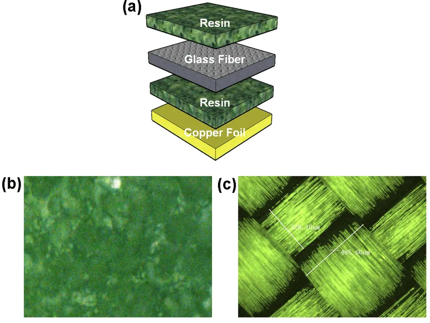
Here's an illustrative image depicting the cross-section of a PCB, highlighting the microstrip and stripline structures critical for 50 ohm impedance design.
Conclusion: Achieving precision with 50 ohm impedance control for robust PCB performance
Mastering stackup design for 50 ohm impedance control is an indispensable skill for engineers engaged in high-frequency and RF applications. By thoroughly understanding the fundamentals of microstrip impedance calculation, stripline impedance design, and judicious PCB material selection, you can craft reliable and efficient designs that consistently meet stringent performance criteria. A meticulously planned impedance control layer stack, supported by accurate calculations and the selection of appropriate materials, is crucial for ensuring signal integrity and minimizing detrimental losses within your circuits.
Begin your design process by clearly defining your stackup configuration, carefully selecting the most suitable materials, and rigorously utilizing simulation tools to validate your design's impedance characteristics before fabrication. With unwavering attention to detail and a steadfast adherence to established best practices, you will be exceptionally well-equipped to navigate and conquer the complexities inherent in 50 ohm impedance PCB design. Cultivate trust in your design methodology, foster collaborative relationships with your manufacturing partners, and strategically leverage the comprehensive insights provided in this guide to significantly elevate the success of your next electronic project.