Introduction
In modern networking infrastructure, router PCBs form the backbone for handling massive data throughput at speeds exceeding 10 Gbps. Ensuring router PCB signal integrity becomes paramount as data rates climb, preventing errors that could disrupt connectivity across enterprise and data center environments. High-speed PCB design demands precise control over electrical characteristics to maintain waveform fidelity from transmitter to receiver. This article explores critical aspects like PCB impedance control, signal reflection minimization, and crosstalk reduction techniques, providing engineers with structured guidance rooted in established principles. By optimizing these elements, designers can achieve reliable high-speed data transfer while adhering to performance benchmarks.

Understanding Signal Integrity in Router PCBs
Signal integrity refers to the preservation of electrical signal quality throughout its propagation across a router PCB. In high-speed environments, degradation from reflections, crosstalk, or attenuation leads to bit errors, increased jitter, and reduced eye diagram margins. For routers processing Ethernet protocols or fiber channel links, maintaining clean signals ensures compliance with timing budgets and BER targets below 10^-12. Factors such as trace geometry, material dielectric properties, and via transitions directly influence integrity. Engineers must analyze these interactions early in the design phase to avoid costly respins. Proper router PCB signal integrity practices enable scalable performance in dense, multilayer boards.
Why Signal Integrity Matters for High-Speed Router Applications
High-speed data transfer in routers amplifies vulnerabilities to signal distortions, where even minor mismatches cascade into system failures. Impedance discontinuities cause reflections that superimpose on incoming signals, narrowing the eye opening and violating setup-hold times. Crosstalk couples noise between adjacent traces, injecting unwanted energy that elevates error rates during bursty traffic. In multilayer router PCBs, power plane interactions and return path disruptions further complicate integrity. Addressing these ensures robust operation under varying loads and temperatures. Ultimately, optimized designs support future-proofing against evolving standards for 25G and beyond.
Fundamental Principles of High-Speed PCB Design
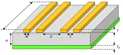
High-speed PCB design relies on transmission line theory, treating traces as controlled-impedance waveguides rather than simple wires. Characteristic impedance, defined by trace width, thickness, dielectric height, and material constants, must match source and load for maximum power transfer. Rise times below 100 ps demand sub-nanosecond precision in routing to stay within the 1/10 wavelength rule for lumped approximations. Differential signaling, common in router SERDES lanes, requires symmetric pair geometries to balance common-mode rejection. Ground and power planes provide low-inductance return paths, stabilizing voltage references. These principles form the foundation for router PCB signal integrity.
Implementing PCB Impedance Control in Router Designs
PCB impedance control involves specifying and verifying trace geometries to achieve target values, typically 50 ohms single-ended or 100 ohms differential for router interfaces. Stackup planning dictates dielectric thicknesses between signal layers and reference planes, with tighter coupling reducing losses. Simulations predict impedance variations from fabrication tolerances like copper roughness or etch factors. Manufacturing feedback loops confirm targets within +/-10% tolerance. IPC-2141 provides guidelines for high-speed controlled impedance circuit boards, emphasizing design verification methods. Consistent control across the board minimizes insertion loss at frequencies above 10 GHz.
Engineers select low-loss dielectrics with stable Dk and Df over frequency, arranging layers to isolate high-speed signals from slower nets. Via stubs introduce discontinuities, so back-drilling or blind vias maintain continuity. Length matching for differential pairs preserves skew below 10 ps. Field solvers validate designs pre-layout, correlating with TDR measurements post-fabrication. This systematic approach ensures high-speed PCB design reliability.
Strategies for Signal Reflection Minimization
Signal reflection minimization starts with matching trace impedance to driver output and receiver input impedances, eliminating voltage standing waves. Discontinuities like bends, T-junctions, or unterminated stubs reflect energy backward, ringing the signal. Serpentine routing or meanders equalize lengths without introducing excess capacitance. Source termination with series resistors or parallel RC networks absorbs backward waves. For routers, AC coupling capacitors in differential lines prevent DC offsets while preserving AC balance. Avoiding vias in critical paths or using optimized stub lengths below quarter-wavelength cutoff limits impacts.
Pre-emphasis and equalization at transceivers compensate for residual effects, but PCB-level fixes provide deterministic performance. IPC-2221 outlines routing guidelines supporting signal integrity through spacing and layer sequencing. Simulations quantify return loss below -20 dB across the bandwidth. Fabricated boards undergo VNA sweeps to confirm S11 parameters. These techniques collectively safeguard high-speed data integrity.
Crosstalk Reduction Techniques in Multilayer Router PCBs
Crosstalk reduction techniques focus on decoupling aggressor and victim traces through spatial and temporal separation. Increasing edge-to-edge spacing beyond 3x trace width suppresses near-end and far-end coupling by reducing mutual inductance and capacitance. Orthogonal routing on adjacent layers minimizes parallel run lengths, slashing capacitive coupling. Guard traces grounded at intervals shield sensitive nets, diverting induced currents. Solid reference planes beneath signals return currents locally, confining loop areas.
Staggered vias and moats in planes interrupt unwanted paths. Differential routing benefits from tight pair spacing and loose neighbor gaps. IPC-6012 specifies performance criteria for rigid boards, including conductor quality affecting coupling. Frequency-domain analysis predicts NEXT and FEXT below -40 dB. Post-layout extraction refines predictions. These methods ensure clean signals in dense router layouts.
Layer Stackup and Routing Best Practices
Optimal layer stackup pairs high-speed signals with adjacent ground planes for symmetric fields and EMI containment. Alternating signal-ground-signal sequences minimizes intra-pair skew. Core and prepreg selection balances thickness control with thermal expansion matching per IPC guidelines. Routing high-speed nets first reserves preferred layers, avoiding splits or gaps in references. Differential pairs maintain constant separation using length-tuning algorithms. Vias transition layers with minimal stub exposure via blind or buried types.
Power distribution networks decouple with stitching vias every lambda/20. Thermal vias under high-power ICs prevent hotspots distorting dielectrics. DFM checks verify clearances for fabrication. Signal integrity co-simulation integrates PDN effects. These practices yield production-ready high-speed PCB designs.
Advanced Considerations for Router PCB Performance
Beyond basics, via optimization using elliptical shapes or density-controlled farms reduces parasitic capacitance. Material selection favors low-Tg laminates for HDI routers, maintaining stability under reflow. Power integrity ties into signal paths via PDN impedance targets below 10 mOhm at GHz frequencies. Eye diagram closure verifies margins post-simulation. Field testing with protocol analyzers confirms link budgets. Iterative refinement bridges design and validation.
Conclusion
Designing router PCBs for optimal signal integrity demands mastery of high-speed PCB design principles, from PCB impedance control to signal reflection minimization and crosstalk reduction techniques. Structured approaches, guided by standards like IPC-2141 and IPC-2221, ensure waveforms remain pristine amid rising data rates. Engineers benefit from early stackup planning, precise routing, and verification loops to deliver reliable networking hardware. Implementing these strategies minimizes risks, accelerates time-to-market, and supports scalable performance. Prioritizing these elements positions designs for long-term success in demanding applications.
FAQs
Q1: What role does PCB impedance control play in router PCB signal integrity?
A1: PCB impedance control ensures traces match driver and receiver characteristics, preventing mismatches that degrade signals at high speeds. Proper stackup and geometry maintain 50/100 ohm targets, reducing insertion loss and enabling clean eye openings. Simulations and TDR tests verify compliance, aligning with IPC-2141 guidelines for controlled impedance. This foundation supports reliable data transfer in routers.
Q2: How can engineers minimize signal reflections in high-speed PCB design?
A2: Engineers minimize signal reflections by matching impedances, avoiding stubs, and using termination resistors. Routing avoids sharp bends and unnecessary vias, while back-drilling cleans transitions. Differential pairs require symmetric layouts for balance. Pre-layout simulations predict S11, with post-fab VNA confirmation. These steps preserve waveform integrity for router applications.
Q3: What are effective crosstalk reduction techniques for router PCBs?
A3: Effective crosstalk reduction techniques include wider trace spacing, orthogonal routing on layers, and ground plane references. Guard traces and staggered vias further isolate signals. Limiting parallel runs below 1 cm cuts coupling. PDN stitching contains return currents. Analysis targets -40 dB NEXT/FEXT, ensuring high-speed data fidelity in dense boards.
Q4: Why is layer stackup critical for high-speed router PCB design?
A4: Layer stackup is critical as it defines impedance, coupling, and return paths in high-speed router PCB design. Ground-signal pairing reduces radiation and skew. Dielectric choices control losses at GHz frequencies. It influences manufacturability and thermal performance. Optimized stackups per IPC-6012 enable robust signal integrity across channels.
References
IPC-2141A — Design Guide for High-Speed Controlled Impedance Circuit Boards. IPC.
IPC-2221B — Generic Standard on Printed Board Design. IPC.
IPC-6012E — Qualification and Performance Specification for Rigid Printed Boards. IPC, 2017.