Introduction
Electronic hobbyists often push their custom PCBs to handle higher power levels in projects like LED drivers, motor controllers, or audio amplifiers. Heat buildup can lead to component failures or reduced performance if not managed properly. One effective DIY PCB modification involves adjusting the outer layer copper thickness to enhance PCB heat dissipation. Thicker copper on the outer layers acts as a better heat spreader due to its high thermal conductivity. This guide focuses on practical techniques for home etching PCB processes, including copper pour thermal strategies and simple electroplating methods. By following these steps, hobbyists can achieve noticeable improvements in PCB thermal design without professional equipment.
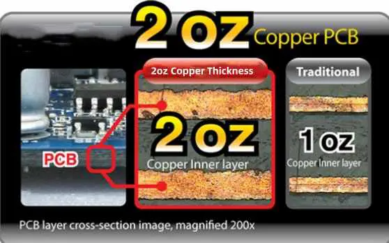
Standard copper clad boards typically feature 1 oz per square foot foil, about 35 micrometers thick. Increasing this to 2 oz or adding plating can significantly boost heat transfer. Copper pours on outer layers provide large surface areas for convection and radiation cooling. Thermal vias connect layers for further dissipation. These modifications align with basic principles from IPC-2152, which guides current-carrying capacity and associated temperature rise. Hobbyists can implement them safely at home with common materials.
Why Modifying Outer Layer Copper Thickness Matters for Hobbyists
Heat dissipation challenges arise in DIY projects where components generate more power than standard designs anticipate. Thin copper layers limit heat spreading, causing hotspots that degrade solder joints or desolder parts during operation. Thicker outer copper improves this by increasing the cross-sectional area for thermal conduction. For instance, power transistors or regulators benefit from direct attachment to beefed-up copper pads. This DIY PCB modification extends component lifespan and allows compact layouts.
In home etching PCB workflows, starting with standard boards means etching defines traces and pours, but thickness remains fixed unless modified. Copper pour thermal areas under hot components spread heat evenly across the board surface. Exposed outer layers cool better than buried inner ones through natural air flow. IPC-6012 outlines performance specs for rigid boards, emphasizing adequate copper for reliability. Hobbyists gain confidence in prototypes that mimic professional thermal management.
Poor thermal design leads to troubleshooting headaches like intermittent failures. Modifying copper thickness addresses root causes proactively. It supports higher currents without excessive temperature rises, per IPC-2152 guidelines. Overall, these changes make DIY projects more robust for real-world use.
Technical Principles of Copper Thickness and PCB Heat Dissipation
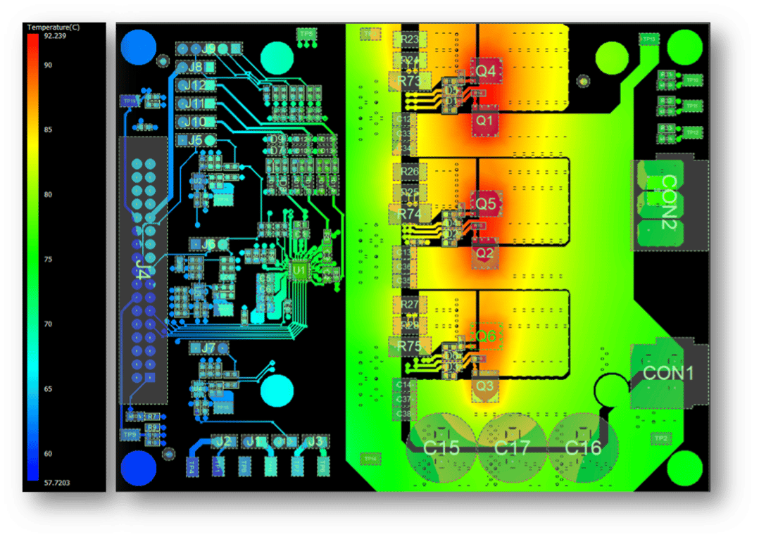
Copper's thermal conductivity, around 400 W/mK, far exceeds FR4 substrate materials. Thicker foils reduce thermal resistance along traces and planes. Heat from a component flows laterally through copper before dissipating upward or via vias. Doubling thickness from 1 oz to 2 oz roughly halves the temperature rise for the same power, based on conduction physics. Surface area matters too; wide copper pours maximize convection.
In PCB thermal design, outer layers excel because they interface directly with ambient air. Radiation and convection dominate here, unlike inner layers insulated by dielectrics. Etch undercut during home etching PCB slightly reduces effective thickness, so starting thicker compensates. Standards like IPC-2152 provide charts correlating copper weight, trace width, current, and delta-T. These help predict performance without simulation tools.
Vias filled with plated copper bridge layers, but outer thickness sets the primary spreading capacity. Impedance to heat flow follows Fourier's law, where path length and area dictate gradients. Hobbyists observe this in IR thermometer tests on prototypes.
Practical DIY Methods for Modifying Outer Layer Copper Thickness
Start with sourcing double-sided 2 oz copper clad FR4 boards, available from hobby suppliers. These have 70 micrometer foil ideal for etching thicker traces directly. Design your layout with generous copper pours around heat sources, connected by wide traces. Use toner transfer or dry film photoresist for precise masks. Etch using ferric chloride at 50 degrees Celsius with bubbling for uniform removal; thicker copper takes 45 to 60 minutes. Rinse, tin if desired, and drill vias.
For further DIY PCB modification, apply post-etch electroplating to thicken existing outer copper. Clean etched boards with acetone and fine sandpaper to expose fresh copper. Prepare a seeding bath using palladium chloride or copper sulfate with hypophosphite reducer for electroless deposition. Dip the board briefly, then thermal treat at 125 degrees Celsius for 10 minutes followed by 175 degrees Celsius for 5 minutes. This seeds holes and surfaces thinly.
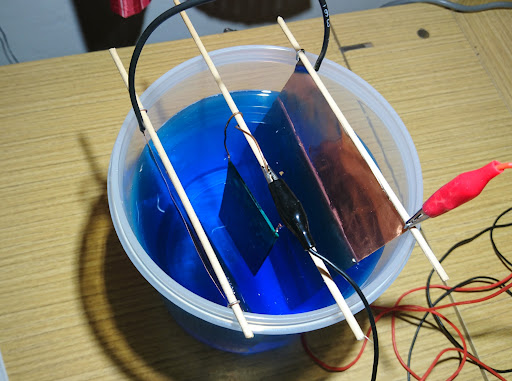
Set up an electroplating tank with copper sulfate electrolyte, sulfuric acid, and a copper anode. Connect the PCB cathode to a 1-3 volt DC supply at low current density, around 10 mA per square cm. Plate for 30-60 minutes to add 20-50 micrometers, agitating for evenness. Rinse thoroughly and dry. This boosts copper pour thermal performance significantly.
Combine with thermal vias: drill 0.3-0.5 mm holes under components, plate during the process. Fill pours avoiding air pockets. Test with a multimeter for continuity and a heat gun for basic thermal checks.
Best Practices and Troubleshooting for Reliable Results
Mask copper pours thoroughly during etching to prevent undercuts exceeding 50% of thickness. Use fresh etchant and monitor temperature to avoid pitting on thicker foils. In electroplating, maintain pH around 1-2 and filter sludge regularly. Uneven plating signals poor seeding; retreat and clean. Overplating risks brittleness, so measure with calipers periodically.
Safety first: work in ventilated areas with gloves and goggles for chemicals. Neutralize waste etchants with baking soda before disposal. Integrate PCB heat dissipation aids like silkscreen labels for airflow paths. Reference IPC-A-600 for visual acceptability criteria post-modification.
Common issues include warped boards from uneven heating; clamp during plating. Blistering indicates contamination; degrease aggressively. These practices ensure hobbyist boards meet basic reliability standards.
Conclusion
Modifying outer layer copper thickness transforms DIY PCBs from fragile prototypes to thermally robust designs. Techniques like using 2 oz clad, copper pours, and home electroplating deliver tangible PCB heat dissipation gains. Hobbyists achieve professional-level PCB thermal design affordably. Key is methodical execution with safety and standards in mind. Experiment iteratively, measuring results to refine future boards. These skills empower endless custom projects.
FAQs
Q1: How does copper pour thermal design improve PCB heat dissipation in home etching PCB projects?
A1: Copper pours create large, low-resistance paths for heat spreading on outer layers. They increase surface area for convection cooling, reducing hotspot temperatures. In DIY setups, fill non-trace areas during layout for maximum effect. Combine with vias for multilayer transfer. This aligns with IPC-2152 principles for temp rise control. Results show cooler operation in power hobby projects.
Q2: What materials are needed for DIY PCB modification via electroplating outer copper?
A2: Gather copper clad boards, copper sulfate, sulfuric acid, hypophosphite or palladium for seeding, DC power supply, and containers. Anode from pure copper sheet, cathode clips for the PCB. Distilled water and agitation tools complete the setup. Start small to test current density. Thickness additions of 20-50 micrometers enhance thermal performance safely at home.
Q3: Can standard 1 oz boards suffice for PCB thermal design after modification?
A3: Yes, post-etch plating effectively thickens them for better heat dissipation. Seed surfaces first for adhesion, then electroplate evenly. Monitor to avoid excess buildup warping thin boards. Copper pours amplify benefits even on base 1 oz. Test with loads mimicking your project. This DIY PCB modification suits most hobbyist needs without sourcing heavy clad.
Q4: What common pitfalls occur in DIY PCB modification for thicker copper?
A4: Uneven etching on thick foils prolongs times, risking mask lift-off. Poor seeding causes patchy plating; ensure clean, oxide-free copper. Overcurrent densities burn deposits. Always ventilate for fumes and neutralize wastes. Follow sequential rinsing to prevent corrosion. Patience yields reliable thermal improvements.
References
IPC-2152A — Standard for Determining Current Carrying Capacity in Printed Board Design. IPC, 2009
IPC-6012E — Qualification and Performance Specification for Rigid Printed Boards. IPC, 2017
IPC-A-600K — Acceptability of Printed Boards. IPC, 2020


