Introduction
High-frequency PCB applications demand surface finishes that preserve signal integrity while ensuring reliable assembly and long-term performance. ENEPIG, or Electroless Nickel Electroless Palladium Immersion Gold, stands out as a preferred choice for these demanding environments due to its multilayer structure that balances solderability, bondability, and electrical stability. Engineers designing RF circuits or high-speed digital interfaces increasingly select ENEPIG for its ability to minimize losses and maintain consistent impedance. This finish addresses common challenges like oxidation and interface degradation seen in simpler coatings. As frequencies push into millimeter-wave ranges, the need for precise control over signal paths becomes critical, making ENEPIG a reliable solution. Its adoption aligns with evolving requirements in telecommunications, automotive radar, and data centers.
What Is ENEPIG and Why It Matters for High-Frequency PCBs
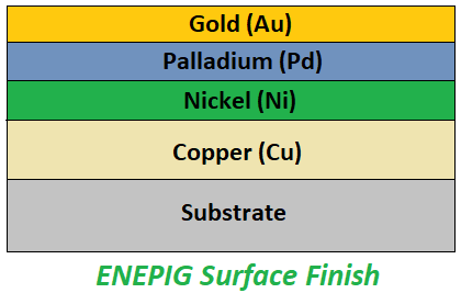
ENEPIG consists of a sequence of electroless nickel, electroless palladium, and immersion gold deposited over copper pads and traces. The nickel layer acts as a diffusion barrier, the thin palladium provides oxidation resistance and interfacial stability, and the gold ensures wettability for soldering. This ternary configuration delivers versatility across multiple assembly processes, including surface-mount technology and wire bonding. Unlike single-layer finishes, ENEPIG offers extended shelf life and resistance to multiple reflow cycles.
In high-frequency contexts, ENEPIG high frequency performance excels because it supports controlled impedance designs up to 40 GHz with reduced interference. Signal paths in RF PCBs and high-speed digital boards experience minimal distortion, as the palladium mitigates nickel's influence on electromagnetic fields. Impedance matching becomes more predictable due to the finish's planarity and uniformity. Engineers value this for applications where even minor variations can degrade performance. Compliance with IPC-4556 ensures consistent quality in production.
The relevance grows with rising data rates and 5G deployments, where traditional finishes falter under skin effect constraints. ENEPIG for RF PCBs provides the electrical uniformity needed for antennas, amplifiers, and transceivers. High-speed digital ENEPIG setups handle gigabit signals without excessive attenuation.
Technical Principles Behind ENEPIG's Superior Performance
At high frequencies, the skin effect confines current to the conductor's outer surface, amplifying losses from surface irregularities or material resistivity. ENEPIG's smooth topography and layered composition counteract this by presenting a low-resistivity gold interface over palladium, which prevents nickel corrosion and diffusion. The palladium barrier maintains interface integrity, avoiding the pitting or black pad issues that plague nickel-gold bilayers. This results in lower ENEPIG signal loss compared to alternatives with rougher nickel exposure. Electrical resistance remains uniform, aiding precise current prediction in traces.
ENEPIG impedance matching benefits from the finish's flatness, which preserves trace geometry and dielectric interactions. Variations in finish thickness or topography can shift characteristic impedance, but ENEPIG's electroless deposition yields consistent coverage on fine-pitch features. In RF designs, this stability supports matching networks and filters. The process adheres to specifications that control layer deposition for repeatability.
Palladium's role extends to high-frequency signal propagation by reducing electromagnetic interference from underlying nickel. At millimeter-wave frequencies, nickel's magnetic properties can introduce losses, but the thin palladium neutralizes this effect. Gold's nobility ensures oxidation-free surfaces post-assembly. Overall, these mechanisms position ENEPIG as optimal for bandwidth-intensive circuits.
Advantages of ENEPIG in High-Frequency Signal Integrity
ENEPIG high frequency performance shines in minimizing insertion loss, particularly where skin depth approaches trace dimensions. The finish's planarity reduces scattering and attenuation, outperforming finishes with thicker or rougher barriers. For instance, in high-speed digital ENEPIG applications, eye diagrams show cleaner openings due to preserved rise times. RF engineers report consistent return loss across boards.
ENEPIG signal loss stays low because the palladium-gold stack presents a favorable conductivity profile to high-frequency currents. Nickel-related RF losses diminish, enabling operation up to 40 GHz without significant degradation. This proves vital for phased arrays and mmWave modules. Compared to nickel-dominant finishes, ENEPIG exhibits lower resistivity at the signal path.
Impedance control in multilayer stacks relies on uniform finishes to avoid modal dispersion. ENEPIG's deposition process ensures even coverage on vias and pads, stabilizing Z0 values. Testing per IPC-6012E confirms performance under thermal stress. High-speed digital ENEPIG thus supports SerDes links and DDR interfaces reliably.
Practical Implementation and Best Practices
Selecting ENEPIG requires specifying deposition per IPC-4556 to guarantee layer integrity and thickness uniformity. Engineers should verify process controls for electroless baths, as variations affect planarity. Pre-production coupons aid qualification, focusing on adhesion and solderability. Multiple reflow simulations mimic assembly conditions.
For ENEPIG for RF PCBs, pair with low-loss dielectrics and controlled roughness bases. Fine-pitch components benefit from the finish's wettability, reducing voids in joints. Quality checks include cross-section analysis for layer continuity. J-STD-001 guidelines support soldering process validation.
Troubleshooting common issues involves monitoring bath chemistry to prevent palladium skips. Shelf life exceeds two years with proper storage, minimizing oxidation risks. In high-volume production, ENEPIG balances cost with performance for mixed RF-digital boards.
Applications in RF and High-Speed Digital PCBs
RF PCBs leverage ENEPIG for front-end modules where low loss and bondability converge. Transceivers and power amplifiers maintain gain with stable matching. High-speed digital ENEPIG suits backplanes and interconnects in servers, preserving signal margins at 56 Gbps PAM4.
Automotive and aerospace sectors adopt it for radar and satcom, enduring harsh environments. The finish's corrosion resistance per IPC standards ensures longevity. Hybrid assemblies with wire bonds thrive on gold wire pull strengths.
Conclusion
ENEPIG emerges as the go-to finish for high-frequency PCB applications through its engineered layers that optimize signal integrity and assembly reliability. Key strengths in ENEPIG high frequency performance, reduced signal loss, and precise impedance matching make it indispensable for RF and high-speed digital designs. Adhering to IPC-4556 and related standards maximizes benefits. Engineers gain confidence in designs pushing frequency limits, supported by proven mechanisms against skin effect and oxidation.
FAQs
Q1: What contributes to ENEPIG high frequency performance in RF PCBs?
A1: ENEPIG high frequency performance stems from its smooth palladium-gold interface, which minimizes skin effect losses and nickel interference up to 40 GHz. The electroless layers ensure planarity for low insertion loss and stable propagation. This suits RF PCBs by preserving gain in amplifiers and antennas. Compliance with IPC-4556 aids consistent results across lots.
Q2: How does ENEPIG signal loss compare in high-speed applications?
A2: ENEPIG signal loss remains low due to the barrier palladium layer negating nickel's high-frequency drawbacks. Uniform resistance supports clean eye patterns in gigabit links. Compared to nickel-exposed finishes, it shows reduced attenuation at mmWave. Engineers prioritize it for high-speed digital ENEPIG to meet bit error rates.
Q3: Why is ENEPIG effective for impedance matching?
A3: ENEPIG impedance matching excels from flat topography and even deposition, avoiding Z0 shifts from roughness. Fine-pitch traces retain geometry integrity. The finish's electrical uniformity aids controlled-impedance stacks per IPC-6012E. This proves critical in RF filter banks and SerDes channels.
Q4: Is ENEPIG suitable for wire bonding in high-frequency boards?
A4: Yes, ENEPIG supports gold and aluminum wire bonding with high pull strength, thanks to the oxide-free nickel surface post-palladium dissolution. It withstands reflow without degradation, ideal for RF hybrids. J-STD-001 validates joint reliability. High-speed digital ENEPIG assemblies benefit from this versatility.
References
IPC-4556 — Specification for Electroless Nickel/Electroless Palladium/Immersion Gold (ENEPIG) Plating for Printed Circuit Boards. IPC
IPC-6012E — Qualification and Performance Specification for Rigid Printed Boards. IPC
J-STD-001H — Requirements for Soldered Electrical and Electronic Assemblies. IPC


