What is a Via Aspect Ratio and Why is it Important for PCBs?
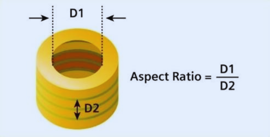
In the intricate world of printed circuit board (PCB) design, the via aspect ratio is a fundamental concept that directly impacts a board's performance and longevity. Essentially, it describes the relationship between a PCB's total thickness and the diameter of a drilled via hole. For example, a 1.6 mm thick board with a 0.2 mm via hole would have an aspect ratio of 8:1.
This ratio is critical because it dictates the ease and quality of copper plating inside the via. Vias act as vital electrical conduits, connecting different layers of a PCB. If the aspect ratio is too high, meaning a very narrow hole through a thick board, proper copper deposition during manufacturing becomes challenging, potentially leading to weak connections, signal degradation, or even catastrophic board failure over time.
How Do You Calculate Via Aspect Ratio?
Determining the via aspect ratio is a straightforward calculation, yet it demands precision to ensure your PCB design is manufacturable and reliable. The process involves two key measurements.
Step-by-Step Calculation
First, measure the overall thickness of your PCB. A common 4 layer circuit board, for instance, might be 1.6 mm thick. Next, ascertain the diameter of the drilled via hole; for through-hole vias, this could typically range from 0.2 mm to 0.5 mm, depending on design specifics. Finally, divide the board's thickness by the via hole diameter. For a 1.6 mm thick board with a 0.3 mm via, the calculation yields an aspect ratio of approximately 5.33:1.
Industry Guidelines and Microvias
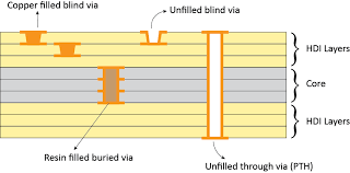
Industry best practices generally suggest maintaining through-hole via aspect ratios between 6:1 and 10:1 to facilitate robust manufacturing. For microvias, which are significantly smaller and commonly found in high-density interconnect (HDI) designs, an ideal aspect ratio is 1:1 or even less to circumvent plating challenges inherent with their miniature size. Adhering to these guidelines helps prevent production problems and ensures long-term operational stability.
What Problems Arise from High Aspect Ratio Vias?
Designing PCBs with a high via aspect ratio—where the board is considerably thicker than the via's diameter—can introduce several significant challenges, compromising overall PCB reliability. While sometimes unavoidable in complex, multi-layer designs, these risks warrant careful consideration.
Plating Difficulties and Thermal Stress
One primary concern is the difficulty in achieving consistent plating. When a via hole is excessively narrow relative to the board's thickness (e.g., a 12:1 ratio), the electroplating solution struggles to penetrate and deposit copper uniformly, often resulting in thinner plating at the via's center—a critical weak point. Furthermore, high aspect ratio vias are more susceptible to cracking when subjected to thermal expansion and contraction during soldering or operational temperature cycles. A via with a 15:1 ratio on a 2.4 mm board, for instance, could develop barrel cracks that disrupt electrical connectivity.
Signal Integrity and Manufacturing Costs
Beyond structural issues, high aspect ratio vias can negatively impact signal integrity in high-frequency applications. Uneven plating or structural imperfections can lead to impedance mismatches, causing signal reflections or losses, with impedance variations potentially reaching 10-15%. From a manufacturing perspective, pushing the boundaries of aspect ratio often necessitates specialized drilling and plating techniques, which inevitably escalate production costs and extend lead times. To mitigate these issues, designers should aim for moderate aspect ratios or collaborate closely with their fabrication partners if high ratios are essential, considering advanced techniques like laser drilling for microvias.
How Do Via Plating Issues Affect PCB Reliability?
The quality of copper plating within a via is paramount for PCB reliability. Defects arising from plating issues can transform an otherwise sound design into a product prone to failure. These problems are often closely linked to the via aspect ratio.
Common Plating Problems
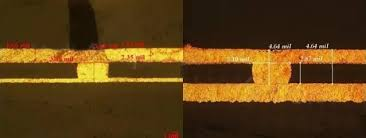
Uneven copper deposition is a frequent issue in high aspect ratio vias, where the plating solution struggles to reach the center of the hole, leading to thinner copper walls. This creates vulnerable points that can fracture under mechanical or thermal stress. Additionally, voids—empty spaces within the copper layer caused by trapped air or contaminants—can significantly reduce conductivity and lead to localized overheating, potentially increasing temperatures by 20-30°C in high-current scenarios.
Impact of Insufficient Plating and Cracking
Industry standards, such as IPC-6012, typically mandate a minimum plating thickness of 20-25 micrometers for reliable vias. Achieving this thickness becomes problematic with excessively high aspect ratios, resulting in subpar electrical performance. Poorly plated vias are also highly susceptible to barrel cracking—fractures along the cylindrical wall—especially in environments involving temperature cycling, where thermal expansion and contraction repeatedly stress the via structure. Mitigating these issues largely depends on optimizing the aspect ratio during the design phase and collaborating with manufacturers employing advanced plating technologies, such as pulse plating, to improve copper distribution even in challenging vias.
Best Practices for Optimizing Via Aspect Ratio in Design
To enhance PCB reliability and avoid the pitfalls associated with problematic via aspect ratios, designers can implement several best practices. These strategies focus on balancing manufacturability with performance objectives.
Adhering to Recommended Ratios and Adjusting Dimensions
A fundamental practice is to design through-hole vias with an aspect ratio between 6:1 and 10:1, while microvias should ideally be at or below 1:1. These ranges represent a sweet spot for manufacturing and operational integrity. If an initial design yields an unfavorably high aspect ratio, consider design modifications such as reducing the board thickness by using fewer layers or, more simply, increasing the via diameter. For example, expanding a via diameter from 0.2 mm to 0.3 mm on a 1.6 mm board significantly reduces the aspect ratio from 8:1 to 5.33:1, simplifying the plating process.
Utilizing Advanced Vias and Simulation
For designs demanding high component density or numerous layers, incorporating microvias—often created with laser drilling—is an excellent strategy. Their inherently low aspect ratios minimize plating challenges. Furthermore, leveraging simulation tools to predict via behavior under various thermal and electrical loads is crucial before finalizing a design. This helps ensure consistent impedance (e.g., within ±10% of a 50-ohm target for RF applications) and prevents signal integrity issues. Finally, proactive communication with your online PCB manufacturer is indispensable. Understanding their specific capabilities and limitations regarding aspect ratios can prevent costly redesigns and production delays, tailoring your design to their expertise.
How Via Aspect Ratio Influences Different PCB Applications
The significance of via aspect ratio is not universal; its impact varies considerably depending on the specific application for which the PCB is designed. Understanding these differences allows for tailored design choices.
High-Frequency and Power Applications
In high-frequency circuits, such as RF or microwave designs, vias must maintain extremely consistent impedance to prevent detrimental signal reflections. High aspect ratios can severely disrupt this consistency, potentially causing signal losses of 3-5 dB in extreme scenarios. For power electronics, which carry substantial currents, robust vias are essential to prevent overheating. Poorly plated, high aspect ratio vias might fail under loads as low as 2-3 amps, risking component burnout.
Consumer, Automotive, and Aerospace Electronics
For compact consumer devices with thin boards, microvias with low aspect ratios are often favored to conserve space while preserving reliability. Conversely, the automotive and aerospace sectors demand vias capable of enduring harsh environmental conditions, including extreme temperatures and vibrations. In these critical applications, a moderate aspect ratio is vital to ensure vias remain structurally sound after numerous thermal cycles, for instance, over 1,000 cycles between -40°C and 125°C. Tailoring via design parameters to the specific demands of the application is key to achieving optimal and lasting reliability.
The Final Word on Mastering Via Aspect Ratio for Dependable PCBs
In the intricate realm of PCB engineering, seemingly minor details can profoundly influence the overall success and reliability of a product. The via aspect ratio, though often understated, stands as a cornerstone of dependable PCB design. By thoroughly understanding how to calculate this ratio, recognizing and mitigating the challenges posed by high aspect ratios, and proactively addressing potential via plating issues, engineers can craft boards that not only perform flawlessly but also endure over time.
Begin by integrating via aspect ratio calculations into the early stages of your design process, aiming for the recommended ranges—typically 6:1 to 10:1 for through-hole vias. Remain vigilant for the inherent problems associated with high ratios, such as plating inconsistencies or increased susceptibility to thermal stress, and proactively apply best practices to refine your design. Whether the end application involves sensitive high-frequency circuits or robust automotive systems, a meticulously designed via can ultimately be the deciding factor between a product's enduring success and its premature failure.


