What is Trace-to-Pad Clearance in PCB Design?
When embarking on the design of a printed circuit board (PCB), one of the most vital considerations is the spacing between conductive elements, such as traces and pads. Trace-to-pad clearance, which refers to the distance separating a conductive trace from a pad, is fundamental to ensuring the PCB's reliability, operational safety, and overall performance. This comprehensive guide will explore the core aspects of trace-to-pad clearance, including minimum spacing requirements, adherence to industry benchmarks like IPC 2221, and practical strategies for optimizing your PCB layout.
At its essence, trace-to-pad clearance signifies the minimum necessary distance between a conductive trace and a pad to avert electrical issues like short circuits, arcing, or signal interference. This specific spacing is determined by various factors, including the operational voltage levels, prevailing environmental conditions, and the capabilities of the manufacturing process. By strictly following established guidelines, such as those detailed in IPC 2221 standards, designers can guarantee the safety and functionality of their PCB designs.
Defining Trace-to-Pad Distance
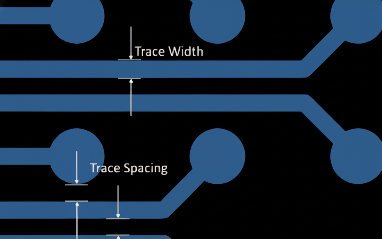
Trace-to-pad clearance is the physical gap between a conductive trace—an electrical pathway on a PCB—and a pad, which is the metallic area designated for component soldering. This spacing is critically important because it actively prevents unintended electrical connections, significantly reduces the likelihood of electrical arcing in high-voltage circuits, and minimizes signal crosstalk in high-speed applications. Without appropriate clearance, a PCB can suffer from short circuits, degraded signal integrity, or even complete operational failure.
In practical terms, the required trace-to-pad distance is affected by the voltage differential between the trace and pad, the operational environment (e.g., humidity or altitude), and the PCB's intended application. For instance, a low-voltage consumer device might tolerate a clearance of just 0.2 mm, whereas a high-voltage industrial system could demand 2.5 mm or more to effectively prevent arcing. Understanding and correctly applying the appropriate minimum trace-to-pad spacing is a foundational skill for any PCB designer aiming for robust and dependable designs.
Why is Trace-to-Pad Spacing Crucial for PCB Reliability?
The importance of maintaining correct trace-to-pad spacing cannot be overstated, as it directly impacts several key aspects of PCB design and long-term functionality.
Impact on Safety, Signal Integrity, and Manufacturability
● Safety: In designs involving high voltages, insufficient clearance can lead to dangerous electrical arcing. This poses a significant risk of fire or severe damage to components. Proper spacing is a fundamental safety measure, preventing such hazardous events.
● Signal Integrity: For high-speed digital circuits, closely spaced traces and pads can induce crosstalk, where electrical signals interfere with each other, leading to data corruption and errors. Adequate clearance minimizes this interference, preserving the integrity of signals.
● Manufacturability: PCB manufacturers operate within specific tolerance limits for spacing. If your trace-to-pad distance is too narrow, the board may be difficult or impossible to fabricate reliably, resulting in production delays, increased costs, or outright defects.
● Reliability: Over time, environmental stressors such as dust accumulation, moisture exposure, or thermal expansion can degrade a PCB's performance. Correct clearance helps reduce the probability of short circuits or system breakdowns under these challenging conditions.
By prioritizing trace-to-pad clearance, designers ensure that their PCBs function reliably throughout their operational lifespan, whether powering a simple consumer gadget or a sophisticated industrial control system.
Understanding IPC 2221 Standards for Trace Spacing
The IPC 2221 standard is a widely recognized and respected guideline in PCB design, providing essential recommendations for trace spacing and clearance. These guidelines are based on varying voltage levels and environmental conditions, helping designers prevent electrical breakdown.
Key Guidelines from IPC 2221
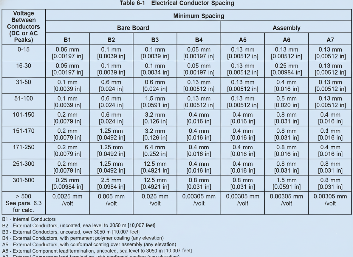
IPC 2221, formally known as the "Generic Standard on Printed Board Design," offers a structured framework for determining safe distances between conductive elements, including trace-to-pad clearance, to prevent electrical failure. According to IPC 2221, the required clearance varies depending on whether the conductors are on the same layer (external) or between different layers (internal), and if they are covered by a protective coating or left uncoated.
Here are some general recommendations from the standard for external conductors operating at sea level:
● Low Voltage: For voltages up to 15V, a minimum clearance of 0.05 mm (2 mils) is typically suggested.
● Moderate Voltage: For voltages ranging between 15V and 30V, the recommended clearance increases to 0.1 mm (4 mils).
● Intermediate Voltage: For voltages between 30V and 50V, a clearance of 0.6 mm (24 mils) is advised.
● High Voltage: For higher voltages, such as 100V to 150V, the required clearance can extend to 1.5 mm (59 mils) or more, depending on the specific application and environmental conditions.
These values serve as initial guidelines and may necessitate adjustments based on factors like altitude (as lower air pressure increases arcing potential) or the presence of protective coatings. IPC 2221 also distinguishes between clearance (the air gap distance) and creepage (the surface distance along the board), both of which are critical considerations for trace-to-pad spacing in high-voltage designs. While strict adherence to IPC 2221 is not always mandatory for all designs, following these standards represents a best practice for ensuring safety and reliability, especially for commercial or industrial applications.
What Factors Influence Minimum Trace-to-Pad Spacing?
The minimum spacing required between a trace and a pad in a PCB design is determined by several interconnected factors. A thorough understanding of these variables is crucial for selecting the appropriate clearance for any given application.
Critical Variables in Spacing Determination
● Voltage Levels: The voltage differential between a trace and a pad is the primary determinant of clearance. Higher voltages significantly increase the risk of electrical arcing, thereby requiring larger separation distances. For instance, a circuit operating at 500V might need a clearance of 6 mm or more, while a 5V circuit could function safely with just 0.2 mm.
● Environmental Conditions: Ambient factors such as humidity, temperature, and altitude can directly affect the dielectric strength of air and the PCB's insulating material. In high-altitude environments, where air pressure is lower, arcing occurs more readily, necessitating increased clearances. Similarly, high humidity can lead to moisture condensation on the board surface, escalating the risk of short circuits if spacing is inadequate.
● Signal Frequency and Speed: In high-speed designs, typically those with signal frequencies exceeding 100 MHz, electromagnetic interference (EMI) and crosstalk become major concerns. Maintaining sufficient trace-to-pad distance effectively reduces these effects, preserving signal integrity. For example, a high-speed USB signal might require a minimum clearance of 0.3 mm to prevent interference with nearby pads.
● Manufacturing Constraints: PCB fabrication processes have inherent limitations regarding the minimum achievable separation between conductive elements. Most standard manufacturing services can produce clearances as tight as 0.15 mm (6 mils), but any tighter spacing may demand specialized techniques or result in higher production costs. It is always wise to consult your manufacturer’s specific design rules to ensure your chosen trace-to-pad distance is feasible.
● Board Material and Coating: The type of PCB substrate material (e.g., FR-4) and any protective coatings or solder masks applied can also influence clearance requirements. A coated board might allow for slightly reduced spacing because the coating adds an extra layer of insulation, whereas uncoated boards generally necessitate more conservative distances.
How to Effectively Determine and Optimize Trace-to-Pad Distance
Calculating the ideal trace-to-pad distance for your HDI PCB involves a careful balance of safety, performance, and manufacturability. A structured approach ensures that you arrive at the correct clearance for your design.
Step-by-Step Approach to Optimal Spacing
1. Identify Voltage Levels: Begin by determining the maximum voltage difference that will exist between any given trace and pad. Use this value as a reference point for IPC 2221 clearance guidelines or any other relevant industry standards applicable to your project.
2. Assess Environmental Factors: Carefully consider the intended operating environment for your PCB. If the board will be deployed in humid or high-altitude conditions, it is prudent to increase the clearance beyond the basic recommendations to account for reduced dielectric strength.
3. Check Signal Requirements: For designs involving high-speed or high-frequency signals, verify that the chosen clearance is sufficient to prevent crosstalk or electromagnetic interference (EMI). Where necessary, employ simulation tools to model these effects and validate your spacing.
4. Review Manufacturer Guidelines: Always confirm the minimum trace-to-pad spacing capabilities supported by your chosen online PCB manufacturer. Adjust your design if required to align with their specific process tolerances and limitations.
5. Utilize Design Software Rules: Most modern PCB design software platforms offer robust features for setting and enforcing clearance rules. Configure these rules based on net classes or specific component requirements to automatically maintain the desired trace-to-pad distance throughout your layout process.
By diligently following these steps, you can ensure that your design adheres to best practices for PCB clearance, effectively meeting the unique demands and performance needs of your specific project.
Common Mistakes to Avoid
Even seasoned designers can inadvertently make mistakes concerning trace-to-pad spacing. Awareness of these common pitfalls can save considerable time and resources.
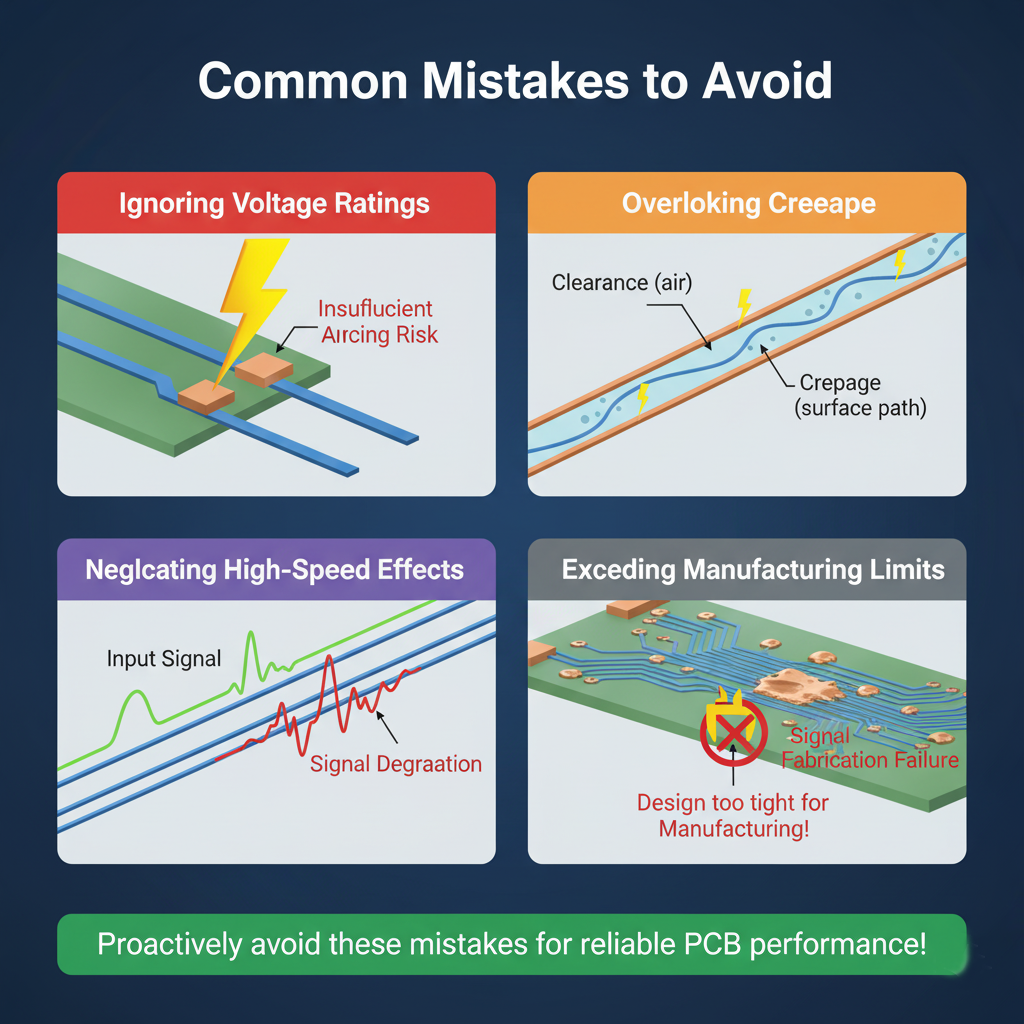
● Ignoring Voltage Ratings: Underestimating the actual voltage differential between a trace and a pad is a frequent error that leads to insufficient clearance, significantly increasing the risk of arcing or short circuits.
● Overlooking Creepage: While clearance (the air gap) is vital, creepage (the surface distance along the board between conductors) is equally, if not more, critical, especially in humid or contaminated environments where surface conductivity can cause shorts.
● Neglecting High-Speed Effects: Failing to account for potential crosstalk in high-speed designs can severely degrade signal quality, even if the voltage-based clearance appears adequate.
● Exceeding Manufacturing Limits: Designing with clearances that are tighter than your manufacturer’s production capabilities will almost certainly result in expensive redesigns, production delays, or outright fabrication failures.
Proactively avoiding these common mistakes will streamline your design process and ensure that your PCB performs precisely as intended.
Practical Optimization Tips
Designing a PCB with optimal trace-to-pad spacing doesn't have to be overly complex. Here are some actionable tips to refine your layout:
● Utilize Design Rule Checks (DRC): Fully leverage the DRC features embedded in your PCB design software. These tools can automatically identify and flag clearance violations during the layout process, catching errors early.
● Group Similar Nets: Strategically place traces and pads that share similar voltage levels or signal types closer together. This minimizes the necessity for excessively large clearances across the entire board, optimizing space.
● Prioritize High-Voltage Areas: Identify and isolate all high-voltage sections of your PCB early in the design phase. Ensure these areas have generously ample clearance from any low-voltage or sensitive sections.
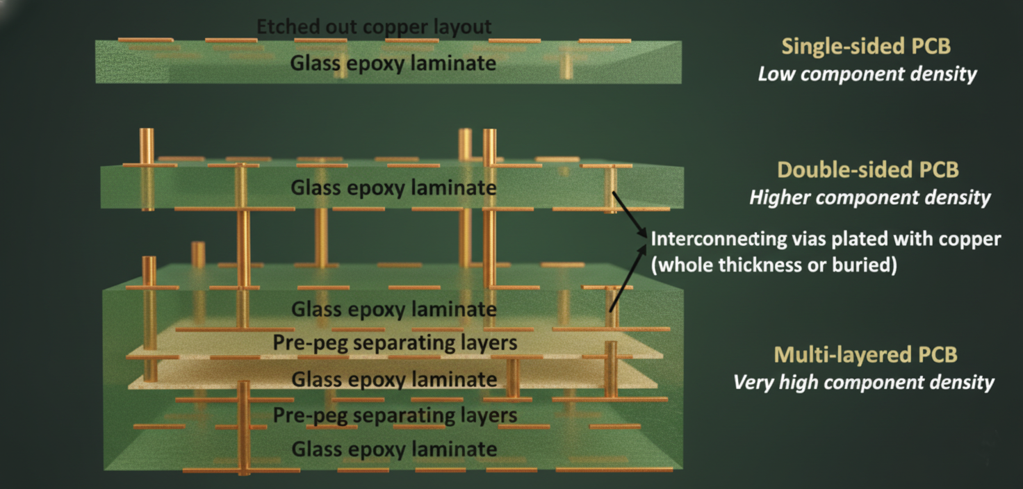
● Consider Multi-Layer Boards: If space constraints become an issue on a single-layer PCB, consider migrating to a multi-layer board. This allows you to effectively separate high-voltage or high-speed traces and pads onto different layers, significantly reducing clearance concerns on any single plane.
● Test and Validate: Upon completing your design, it is crucial to simulate or prototype the PCB. This validation step allows you to verify that the trace-to-pad distances perform as expected under actual real-world operating conditions.
These strategies collectively contribute to creating a robust PCB layout that effectively balances the essential clearance requirements with overall design efficiency.
Conclusion: Mastering Trace-to-Pad Clearance for Superior PCBs
Trace-to-pad clearance is a foundational element of PCB design that directly influences safety, performance, and manufacturability. By thoroughly understanding the significance of trace-to-pad distance, adhering to established industry standards like IPC 2221 trace spacing guidelines, and carefully considering influencing factors such as voltage, environmental conditions, and signal speed, designers can create highly reliable and efficient PCB layouts. Proactively avoiding common design mistakes and implementing practical optimization tips further ensures that your design meets the most stringent quality standards.
Whether your project involves a low-voltage consumer device or a high-voltage industrial system, mastering minimum trace-to-pad spacing is essential for achieving success. With the detailed insights and strategic approaches shared in this guide, you are well-equipped to navigate PCB clearance challenges and deliver designs that demonstrate enduring reliability and performance. By consistently applying these principles in your upcoming projects, you will undeniably recognize the profound impact that proper spacing has on the quality and functionality of your PCBs.


