Introduction
Printed circuit boards (PCBs) play a critical role in radio frequency (RF) applications, where signal integrity and performance are paramount. Selecting the right PCB materials and determining the optimal copper thickness are vital for ensuring conductivity and minimizing signal loss. RF designs often operate at high frequencies, making material properties and copper foil type significant factors in achieving reliable performance. This article delves into the relationship between PCB materials, copper thickness, and design considerations for RF applications. Aimed at electrical engineers, the content provides a detailed exploration of conductivity and design principles, alongside practical insights for optimizing RF circuits. By understanding these elements, engineers can make informed decisions to enhance the efficiency of their designs.
What Are PCB Materials for RF Applications and Why Do They Matter
PCB materials form the foundation of any circuit board, acting as the substrate that supports conductive traces and components. In RF applications, these materials must exhibit specific electrical properties to handle high-frequency signals without degradation. Dielectric constant, loss tangent, and thermal stability are key parameters that influence signal propagation and power handling. Materials with low dielectric loss are preferred to reduce energy dissipation, while a stable dielectric constant ensures consistent performance across frequencies.
The importance of material selection in RF applications cannot be overstated. Poor choices can lead to signal attenuation, phase distortion, or impedance mismatches, all of which degrade system performance. Additionally, the interaction between the substrate and copper foil affects the overall conductivity and design outcomes. Engineers must balance these factors to meet the stringent demands of RF systems, such as those in telecommunications, radar, and wireless devices.
Technical Principles of Copper Thickness in RF Design
Copper thickness on a PCB directly impacts its electrical and thermal performance, especially in RF applications. The conductive layer, typically made of copper foil, carries signals across the board. In high-frequency designs, the skin effect becomes a dominant factor. This phenomenon causes current to flow primarily on the surface of the conductor, reducing the effective cross-sectional area for current flow. As frequency increases, the skin depth decreases, meaning thinner copper layers can still conduct effectively if designed properly.
Standard copper thicknesses for PCBs range from 0.5 oz/ft2 to 2 oz/ft2, with higher thicknesses used for power handling. However, in RF applications, thicker copper may not always be beneficial due to increased surface roughness, which can exacerbate signal loss. Conductivity and design must account for this trade-off. Smoother copper foil types are often selected to minimize loss at high frequencies, as roughness can introduce parasitic effects.
Another principle to consider is impedance control. Copper thickness influences the characteristic impedance of transmission lines, a critical parameter in RF circuits. Variations in thickness can lead to mismatches, affecting signal integrity. Standards such as IPC-2221B provide guidelines for designing conductor thickness to meet impedance requirements. Engineers must also evaluate thermal dissipation, as thicker copper can improve heat spreading but may complicate manufacturing processes.
Influence of PCB Copper Foil Type on RF Performance
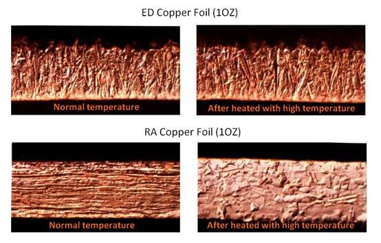
Not all copper foils are created equal, especially when it comes to RF applications. The type of copper foil used in PCB manufacturing significantly affects signal performance. Two primary categories exist: electrodeposited (ED) copper and rolled annealed (RA) copper. ED copper, commonly used in standard PCBs, has a rougher surface due to its manufacturing process. This roughness can increase signal loss at high frequencies, making it less ideal for RF designs.
In contrast, RA copper offers a smoother surface, reducing skin effect losses and improving signal integrity. This type of foil is often preferred in RF applications where minimizing attenuation is crucial. Some specialized foils undergo additional treatments to further enhance surface smoothness, aligning with the needs of high-frequency designs. Selecting the appropriate PCB copper foil type requires understanding the frequency range of the application and the material's interaction with the substrate.
Surface finish also plays a role. Treatments like chemical smoothing or specific plating processes can optimize the copper surface for RF performance. Engineers must consult industry standards, such as IPC-4562A, which specifies requirements for copper foil used in printed boards, to ensure compatibility with design goals.
Practical Solutions for Optimizing Copper Thickness in RF PCBs
Achieving optimal copper thickness for RF applications involves a systematic approach to material selection and design. Below are actionable strategies to guide engineers in this process:
- Evaluate Frequency Range: Determine the operating frequency of the RF circuit. Higher frequencies often benefit from thinner copper due to the skin effect. Use simulation tools to model signal behavior and identify the ideal thickness.
- Select Suitable Materials: Choose substrates with low dielectric loss and stable properties across the target frequency range. Match the material's characteristics with the copper foil type to minimize signal degradation.
- Adhere to Impedance Requirements: Follow guidelines from standards like IPC-2221B to calculate conductor dimensions for controlled impedance. Ensure manufacturing tolerances align with design specifications.
- Consider Thermal Needs: Assess the power dissipation requirements of the circuit. Thicker copper may be necessary for high-power RF applications to manage heat, but balance this with potential signal loss.
- Test and Validate: Prototype designs with varying copper thicknesses and foil types. Measure performance metrics such as insertion loss and return loss to confirm the design meets expectations.
Collaboration between design and manufacturing teams is essential to ensure that the chosen copper thickness and foil type can be consistently produced. Specifications outlined in IPC-6012E for rigid printed boards provide a framework for quality and performance validation during manufacturing.
Related Reading: Core Thickness for RF PCBs: Minimizing Signal Loss in Wireless Applications
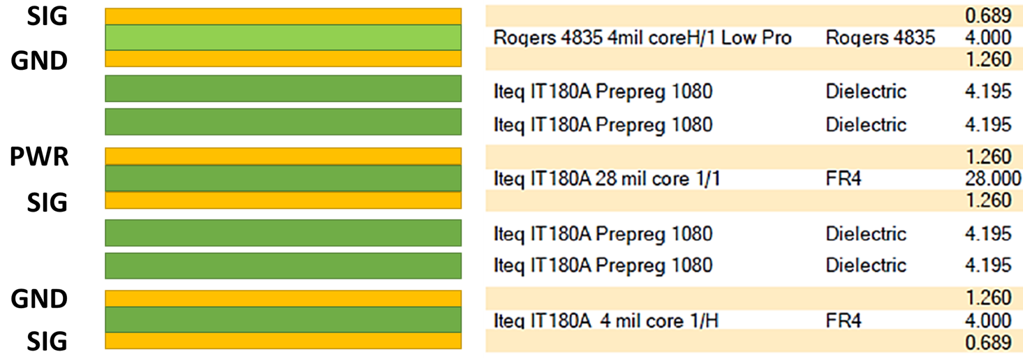
Material and Copper Thickness Interactions in RF Design
The interaction between PCB materials and copper thickness is a critical aspect of RF design. Substrates with high dielectric constants can reduce the physical size of transmission lines, but they may also increase signal loss if not paired with appropriate copper thickness. Conversely, low dielectric constant materials allow for wider traces, potentially requiring thicker copper to maintain conductivity and design integrity.
Related Reading: Understanding the Dielectric Constant of RF Laminate PCBs: A Beginner's Guide
Thermal expansion differences between the substrate and copper layer must also be considered. Mismatches can lead to mechanical stress, especially in high-frequency environments with rapid temperature changes. Standards such as IPC-TM-650 provide test methods for assessing thermal properties, helping engineers select compatible material combinations.
Surface roughness of the copper foil interacts with the substrate's surface as well. A rougher copper surface can increase adhesion to the substrate but may degrade signal performance. Engineers must strike a balance, often opting for smoother foils in RF applications while ensuring reliable bonding. Detailed specifications in IPC-4562A offer guidance on acceptable roughness parameters for copper foils used in such designs.
Conclusion
Designing PCBs for RF applications requires careful consideration of materials and copper thickness to achieve optimal performance. The choice of substrate, copper foil type, and conductor thickness directly influences conductivity and design outcomes, particularly in high-frequency environments. By understanding technical principles such as the skin effect and impedance control, engineers can make informed decisions to minimize signal loss and enhance reliability. Practical strategies, grounded in industry standards like IPC-2221B and IPC-4562A, provide a roadmap for balancing electrical and thermal requirements. Ultimately, a thorough approach to material selection and design validation ensures that RF circuits meet the demanding needs of modern applications.
FAQs
Q1: What are the key PCB materials to consider for RF applications?
A1: For RF applications, PCB materials with low dielectric loss and stable dielectric constants are essential. These properties help minimize signal attenuation and ensure consistent performance at high frequencies. Materials must also offer thermal stability to withstand operating conditions. Engineers should refer to industry standards like IPC-4101E for guidance on selecting substrates that align with specific RF design needs.
Q2: How does copper thickness affect conductivity and design in RF circuits?
A2: Copper thickness impacts conductivity and design by influencing signal loss and impedance in RF circuits. Due to the skin effect, thinner copper may suffice at higher frequencies, but it must balance with thermal dissipation needs. Standards such as IPC-2221B provide formulas for calculating appropriate thickness to maintain signal integrity and meet design requirements.
Q3: Which PCB copper foil type is best suited for high-frequency RF applications?
A3: Rolled annealed copper foil is often preferred for high-frequency RF applications due to its smoother surface, which reduces signal loss from the skin effect. Electrodeposited copper, with a rougher texture, may introduce more attenuation. Consulting IPC-4562A ensures the selected foil meets performance criteria for specific RF designs.
Q4: Why is impedance control critical in RF PCB design with varying copper thickness?
A4: Impedance control is vital in RF PCB design to prevent signal reflections and ensure efficient power transfer. Copper thickness directly affects the characteristic impedance of transmission lines. Variations can lead to mismatches, degrading performance. Adhering to guidelines in IPC-2221B helps engineers design conductors for precise impedance matching in RF applications.
References
IPC-2221B — Generic Standard on Printed Board Design. IPC, 2012.
IPC-4562A — Metal Foil for Printed Board Applications. IPC, 2008.
IPC-6012E — Qualification and Performance Specification for Rigid Printed Boards. IPC, 2020.
IPC-4101E — Specification for Base Materials for Rigid and Multilayer Printed Boards. IPC, 2017.
IPC-TM-650 — Test Methods Manual. IPC, Current Version.


